Choose your country or region.

Image may be representation.
See specs for product details.

TPS61093DSK

In Stock 99400 pcs Reference Price(In US Dollars)
1+
$1.0944
Manufacturer Part Number:
TPS61093DSK
Manufacturer / Brand
TI
Part of Description:
1087
Datasheets:
Lead Free Status / RoHS Status:
RoHS Compliant
Stock Condition:
New original, 99400 pcs Stock Available.
ECAD Model:
Ship From:
Hong Kong
Shipment Way:
DHL/Fedex/TNT/UPS

Inquiry Online

Please complete all required fields with your contact information.Click "SUBMIT REQUEST" we will contact you shortly by email. Or Email us: Info@IC-Components.com
Part Number
Manufacturer
Require Quantity
Target Price(USD)
Company Name
Contact Name
E-mail
Phone
Message
Please enter Verify Code and click "Submit"
Part Number TPS61093DSK
Manufacturer / Brand TI
Stock Quantity 99400 pcs Stock
Category Integrated Circuits (ICs) > Specialized ICs
Description 1087
Lead Free Status / RoHS Status: RoHS Compliant
RFQ TPS61093DSK Datasheets TPS61093DSK Details PDF
TPS61093DSK Details PDF for FR.pdf
TPS61093DSK Details PDF for KR.pdf
TPS61093DSK Details PDF for DE.pdf
TPS61093DSK Details PDF for IT.pdf
TPS61093DSK Details PDF for ES.pdf
Condition New Original Stock
Warranty 100% Perfect Functions
Lead Time 2-3days after payment.
Payment Credit Card / PayPal / Telegraphic Transfer (T/T) / Western Union
Shipping by DHL / Fedex / UPS / TNT
Port HongKong
RFQ Email Info@IC-Components.com

Packaging & ESD

Industry-standard static shielding packaging is used for electronic components.Anti-static, light-transparent materials allow easy identification of ICs and PCB assemblies.
The packaging structure provides electrostatic protection based on Faraday cage principles.This helps protect sensitive components from static discharge during handling and transportation.


All products are packed in ESD-safe anti-static packaging. Outer packaging labels include part number, brand, and quantity for clear identification. Goods are inspected prior to shipment to ensure proper condition and authenticity.

ESD protection is maintained throughout packing, handling, and global transportation. Secure packaging provides reliable sealing and resistance during transit. Additional cushioning materials are applied when required to protect sensitive components.

QC(Part Testing by IC Components)Quality Warranty

We can offer worldwide express delivery service, such as DHLor FedEx or TNT or UPS or other forwarder for shipment.

Global Shipment by DHL/FedEx/TNT/UPS

Shipping Fees reference DHL/FedEx
1). You can offer your express delivery account for shipment, ifyou haven’t any express account for shipment, we can offer our account inadvance.
2). Use our account for shipment, Shipment charges(Reference DHL/FedEx, Different Countries has different price.)
Shipment charges: (Reference DHL and FedEX)
Weight(KG): 0.00kg-1.00kg Price(USD$) : USD$60.00
Weight(KG): 1.00kg-2.00kg Price(USD$) : USD$80.00
* The price of cost is reference with DHL/FedEx. The detail charges, please contact us. Different country the express charges are different.


We accept the payment terms: Telegraphic Transfer(T/T), Credit Card, PayPal and Western Union.

PayPal:

PayPal Bank Information:
Company Name : IC COMPONENTS LTD
Paypal ID: PayPal@IC-Components.com

BANK TRANSFAR (Telegraphic Transfer)

Payment For Telegraphic Transfers:
Company Name : IC COMPONENTS LTD Beneficiary Account Number : 549-100669-701
Beneficiary Bank name : Bank of Communications (Hong Kong) Ltd Beneficiary Bank Code : 382 (for local payment)
Beneficiary Bank SWIFT : COMMHKHK
Beneficiary Bank Address : Tsuen Wan Market Street Branch 53 Market Street, Tsuen Wan N.T., Hong Kong

Any inquires or questions, please kindly contact us Email: Info@IC-Components.com


TPS61093DSK Product Details:

Here's a comprehensive summary description of the TPS61093DSK product:

The TPS61093DSK is a specialized integrated circuit developed by Texas Instruments (formerly Luminary Micro) designed to address power management challenges in compact electronic systems. This high-performance device is specifically engineered to provide efficient voltage conversion and power regulation for sophisticated electronic applications.

As a specialized integrated circuit, the product offers advanced power management capabilities, enabling designers to optimize power efficiency in space-constrained devices. The component is particularly valuable in portable electronics, embedded systems, and applications requiring precise voltage control with minimal footprint.

The circuit's design tackles critical engineering challenges such as power conversion efficiency, thermal management, and compact form factor integration. Its sophisticated architecture allows for seamless voltage transformation while maintaining low power consumption and minimal heat generation.

Key specifications include support for a wide input voltage range and the ability to deliver stable output voltage across diverse operating conditions. The device comes in a compact 1087 encapsulation format, making it ideal for dense electronic designs where space optimization is crucial.

Primary advantages include high reliability, exceptional energy efficiency, and robust performance across varied environmental conditions. The component demonstrates superior power management capabilities, reducing overall system power requirements and enhancing device longevity.

While compatibility depends on specific system requirements, the TPS61093DSK is generally suited for applications in consumer electronics, telecommunications, automotive electronics, and industrial control systems. Its versatile design enables integration into multiple electronic platforms requiring precise power regulation.

Equivalent or alternative models in the Texas Instruments product lineup include the TPS61090, TPS61091, and TPS61092 series, which offer similar power management functionalities with slight variations in voltage handling and specific performance characteristics.

The substantial quantity of 5000 units suggests this is likely a bulk procurement for large-scale manufacturing or extensive product development projects, indicating its significance in industrial and commercial electronic design contexts.

TPS61093DSK Key Technical Attributes

Input Voltage Range: 2.5V to 5.5V

Output Voltage: Adjustable up to 5.5V

Switching Frequency: 1.2 MHz

Maximum Output Current: Up to 600 mA

Efficiency: Up to 95%

Operating Temperature Range: -40°C to 85°C

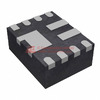
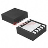
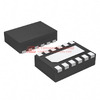
TPS61093DSK Packing Size

Type: Reel packaging suitable for automated assembly

Material: Anti-static carrier tape

Size: Standard 1087 encapsulation size for surface mount devices

Pin Configuration: 8-pin DFN package

Thermal Characteristics: Junction-to-ambient thermal resistance optimized for enhanced heat dissipation

Electrical Properties: Low quiescent current, voltage feedback control, and built-in overcurrent protection

TPS61093DSK Application

The TPS61093DSK is ideal for portable battery-powered applications such as handheld devices, smartphones, PMPs, and other portable consumer electronics requiring efficient step-up DC-DC conversion. It is also suitable for driving LCD bias supplies and powering OLED displays.

TPS61093DSK Features

This integrated circuit features a high-efficiency synchronous boost converter with a fixed 1.2 MHz switching frequency, minimizing external component sizes. It offers an internal synchronous rectifier to reduce power loss, supporting low voltage operation down to 2.5V. Its integrated compensation allows for rapid transient response without the necessity for external compensation components. The IC incorporates multiple protection mechanisms including thermal shutdown, undervoltage lockout, and current limit to enhance robustness. Additionally, the device supports a soft-start function to prevent inrush current during startup and features a shutdown mode to minimize power consumption when inactive.

TPS61093DSK Quality and Safety Features

Manufactured by Texas Instruments, the TPS61093DSK complies with rigorous quality assurance standards including AEC-Q100 automotive qualification. The device undergoes comprehensive testing to ensure reliability under harsh environmental conditions. It incorporates built-in fault detection and protection circuits such as overtemperature protection and short-circuit prevention to maintain safe operation.

TPS61093DSK Compatibility

The TPS61093DSK is compatible with standard 8-pin PCB layouts in the DFN package family, enabling easy replacement in existing designs. It interfaces seamlessly with common microcontroller-based systems requiring regulated step-up voltage supplies. It supports a wide range of input voltages allowing integration into various battery chemistries including NiMH, Li-ion, and alkaline cells.

TPS61093DSK Datasheet PDF

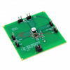
Our website hosts the most authoritative and up-to-date datasheet for the TPS61093DSK from Texas Instruments. Customers are highly encouraged to download the datasheet directly from this page to access detailed electrical characteristics, application circuits, design guidelines, and typical performance charts critical for optimal system design.

Quality Distributor

IC-Components is your trusted premium distributor for Texas Instruments products including the TPS61093DSK. We guarantee genuine components backed by reliable sourcing and prompt service. Visit our website to request a competitive quote and leverage our expansive inventory to support your production needs with confidence and speed.

Frequently Asked Questions

Can the TPS61093DSK boost converter be used in a 3.3V-to-5V power supply design for an industrial sensor node with intermittent high-current loads?
Yes, the TPS61093DSK is well-suited for 3.3V-to-5V step-up applications with pulsed loads typical of industrial sensor nodes. Its integrated 1.2A switch current limit and low quiescent current (typically 25 µA) support efficient operation during both idle and burst modes. However, ensure input capacitance is sufficient to handle load transients, and verify that peak inductor current does not exceed 1.5A under worst-case duty cycle conditions to avoid saturation.
What are the critical layout considerations when designing a PCB with the TPS61093DSK to minimize EMI and ensure stable switching performance?
Minimize the high-di/dt loop formed by the input capacitor, inductor, and SW pin by placing these components as close as possible to the TPS61093DSK. Use a solid ground plane beneath the IC and keep feedback traces (FB pin) away from noisy switching nodes. A 10–22 µF low-ESR ceramic input capacitor placed within 3 mm of VIN and GND pins is essential to suppress voltage ripple and reduce conducted emissions.
Is the TPS61093DSK a drop-in replacement for the MAX756 in a legacy 2-cell alkaline to 3.3V design, and what modifications might be needed?
The TPS61093DSK can replace the MAX756 in many 2-cell alkaline to 3.3V applications due to similar input voltage range (0.7V–5.5V) and output capability, but it is not a true drop-in. Key differences include higher switching frequency (1.2 MHz vs. ~30 kHz), requiring a smaller inductor, and different feedback thresholds. You must recalculate feedback resistor values and verify stability with your chosen output capacitor ESR, as the TPS61093DSK requires <1 Ω ESR for optimal transient response.
How does the enable/shutdown behavior of the TPS61093DSK affect system power sequencing in battery-powered IoT devices?
The TPS61093DSK features a logic-controlled EN pin with a typical threshold of 0.8V (high) and 0.4V (low), enabling direct interfacing with microcontroller GPIOs. In shutdown, the device draws less than 1 µA, making it ideal for battery-powered IoT systems. However, note that the output remains floating during shutdown—add a bleed resistor (e.g., 100 kΩ) from VOUT to GND if downstream circuits require defined logic states when powered off.
Can the TPS61093DSK operate reliably in an automotive under-hood environment with ambient temperatures up to 105°C?
The TPS61093DSK is rated for operation from –40°C to +85°C junction temperature, which may be exceeded in sustained 105°C ambient conditions without significant derating. While short-term excursions are manageable, continuous operation above 85°C ambient risks thermal shutdown or reduced lifetime. For automotive under-hood use, consider adding a small heatsinking copper area on the PCB or selecting a higher-temperature-rated alternative like the TPS61094 (125°C rated).
What output voltage accuracy can be expected from the TPS61093DSK when using standard 1% tolerance feedback resistors, and how does line/load regulation impact this in precision analog supply applications?
With 1% feedback resistors, the total output voltage accuracy of the TPS61093DSK is approximately ±3.5%, dominated by the ±1.5% internal reference tolerance and resistor errors. Combined with typical line regulation of 0.02%/V and load regulation of 0.5%, this may be insufficient for precision analog rails (e.g., ADC references). For such cases, use 0.1% resistors and consider post-regulation with an LDO if tighter than ±2% regulation is required.
Are there known compatibility issues when paralleling multiple TPS61093DSK devices to increase output current capacity?
The TPS61093DSK is not designed for direct paralleling due to lack of current-sharing mechanisms and synchronized switching. Attempting to parallel units can cause beat frequencies, uneven current distribution, and potential instability. For higher current needs, select a single-device solution with higher current capability (e.g., TPS61088) or use external synchronization and ballast resistors—though the latter reduces efficiency and is not recommended for mass production.
How does the TPS61093DSK handle startup into a pre-biased output voltage, such as during hot-swap or redundant power scenarios?
The TPS61093DSK does not support monotonic startup into a pre-biased output. If VOUT is already present when EN is asserted, the device may experience reverse current through the inductor or erratic regulation until the internal soft-start completes. To avoid latch-up or overshoot, ensure the output is discharged before enabling, or implement an external pre-charge circuit to bring VOUT close to the target voltage before activating the TPS61093DSK.
What inductor characteristics are most critical when selecting a replacement for the recommended 4.7 µH inductor in a space-constrained wearable design using the TPS61093DSK?
Prioritize saturation current (>1.5 A), DC resistance (<100 mΩ), and physical size (e.g., 3×3 mm or smaller). The inductor must maintain inductance above 3 µH at full load to prevent subharmonic oscillation. Avoid molded or shielded types with high DCR, as they reduce efficiency in low-input-voltage wearable applications. Verify stability with your specific Cout and trace inductance using TI’s WEBENCH tool before finalizing the layout.
Does the TPS61093DSK require external compensation components, and how does this simplify or complicate migration from older voltage-mode boost converters?
The TPS61093DSK uses internal compensation, eliminating the need for external RC networks—a significant advantage over older voltage-mode controllers like the LT1302. This simplifies layout and BOM but reduces flexibility in optimizing transient response for non-standard loads. When migrating, focus on matching output capacitor ESR and ensuring the control loop remains stable with your chosen Cout; most ceramic capacitor configurations work without adjustment.

Recent Reviews

Leave Comment
Hello, you have not logged in, please log in
User Login

Forgot password?

No account yet? Register now

Tips
Please speak legally
Your email will be hidden
Please complete all required fields ( denoted with* )
Mark
5.0

You May Also Be Interested In:


TPS61093DSK

TI

1087

In Stock: 99400

SUBMIT RFQ