Choose your country or region.

296~4206244~RTW~24.jpg ImageView larger image
Image may be representation.
See specs for product details.

LMX2485ESQX/NOPB

In Stock 4100 pcs Reference Price(In US Dollars)
1+
$2.9766
10+
$2.9031
30+
$2.8556
100+
$2.8068
Manufacturer Part Number:
LMX2485ESQX/NOPB
Manufacturer / Brand
Texas Instruments
Part of Description:
IC FREQ SYNTH 24WQFN
Datasheets:
LMX2485ESQX/NOPB.pdf
Lead Free Status / RoHS Status:
ROHS3 Compliant
Stock Condition:
New original, 4100 pcs Stock Available.
ECAD Model:
Ship From:
Hong Kong
Shipment Way:
DHL/Fedex/TNT/UPS

Inquiry Online

Please complete all required fields with your contact information.Click "SUBMIT REQUEST" we will contact you shortly by email. Or Email us: Info@IC-Components.com
Part Number
Manufacturer
Require Quantity
Target Price(USD)
Company Name
Contact Name
E-mail
Phone
Message
Please enter Verify Code and click "Submit"
Part Number LMX2485ESQX/NOPB
Manufacturer / Brand Texas Instruments
Stock Quantity 4100 pcs Stock
Category Integrated Circuits (ICs) > Clock/Timing - Clock Generators, PLLs, Frequency Synthesizers
Description IC FREQ SYNTH 24WQFN
Lead Free Status / RoHS Status: ROHS3 Compliant
Voltage - Supply 2.5V ~ 3.6V
Type Frequency Synthesizer (RF)
Supplier Device Package 24-WQFN (4x4)
Series PLLatinum™
Ratio - Input:Output 3:2
Package / Case 24-WFQFN Exposed Pad
Package Tape & Reel (TR)
PLL Yes
Output Clock
Operating Temperature -40°C ~ 85°C
Number of Circuits 1
Mounting Type Surface Mount
Input Clock
Frequency - Max 3GHz
Divider/Multiplier Yes/Yes
Differential - Input:Output Yes/No
Base Product Number LMX2485

Packaging & ESD

Industry-standard static shielding packaging is used for electronic components.Anti-static, light-transparent materials allow easy identification of ICs and PCB assemblies.
The packaging structure provides electrostatic protection based on Faraday cage principles.This helps protect sensitive components from static discharge during handling and transportation.


All products are packed in ESD-safe anti-static packaging. Outer packaging labels include part number, brand, and quantity for clear identification. Goods are inspected prior to shipment to ensure proper condition and authenticity.

ESD protection is maintained throughout packing, handling, and global transportation. Secure packaging provides reliable sealing and resistance during transit. Additional cushioning materials are applied when required to protect sensitive components.

QC(Part Testing by IC Components)Quality Warranty

We can offer worldwide express delivery service, such as DHLor FedEx or TNT or UPS or other forwarder for shipment.

Global Shipment by DHL/FedEx/TNT/UPS

Shipping Fees reference DHL/FedEx
1). You can offer your express delivery account for shipment, ifyou haven’t any express account for shipment, we can offer our account inadvance.
2). Use our account for shipment, Shipment charges(Reference DHL/FedEx, Different Countries has different price.)
Shipment charges: (Reference DHL and FedEX)
Weight(KG): 0.00kg-1.00kg Price(USD$) : USD$60.00
Weight(KG): 1.00kg-2.00kg Price(USD$) : USD$80.00
* The price of cost is reference with DHL/FedEx. The detail charges, please contact us. Different country the express charges are different.


We accept the payment terms: Telegraphic Transfer(T/T), Credit Card, PayPal and Western Union.

PayPal:

PayPal Bank Information:
Company Name : IC COMPONENTS LTD
Paypal ID: PayPal@IC-Components.com

BANK TRANSFAR (Telegraphic Transfer)

Payment For Telegraphic Transfers:
Company Name : IC COMPONENTS LTD Beneficiary Account Number : 549-100669-701
Beneficiary Bank name : Bank of Communications (Hong Kong) Ltd Beneficiary Bank Code : 382 (for local payment)
Beneficiary Bank SWIFT : COMMHKHK
Beneficiary Bank Address : Tsuen Wan Market Street Branch 53 Market Street, Tsuen Wan N.T., Hong Kong

Any inquires or questions, please kindly contact us Email: Info@IC-Components.com


LMX2485ESQX/NOPB Product Details:

The LMX2485ESQX/NOPB from Texas Instruments (Luminary Micro division) is a high-performance RF frequency synthesizer integrated circuit designed to generate precise clock signals for demanding wireless and communication applications. This sophisticated device belongs to the Clock/Timing category, specifically within the Clock Generators, PLLs, and Frequency Synthesizers classification, and is part of the PLLatinum series known for advanced phase-locked loop technology.

This frequency synthesizer addresses critical design challenges in modern RF systems where precise frequency generation, low phase noise, and wide frequency coverage are essential. Operating up to an impressive maximum frequency of 3GHz, the device incorporates an integrated PLL (Phase-Locked Loop) with both divider and multiplier capabilities, offering a flexible 2:56 input-to-output ratio that enables designers to generate a wide range of output frequencies from a single reference clock input. The single-circuit architecture accepts a clock input and produces a clock output, with differential input capability while providing single-ended output, making it versatile for various system architectures.

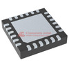
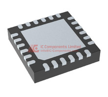
Key specifications include a supply voltage range of 2.5V to 3.6V, making it compatible with modern low-power digital systems, and an operating temperature range of -40°C to 85°C suitable for industrial-grade applications. The device comes in a compact 24-WQFN (4x4mm) package with an exposed pad for enhanced thermal performance, utilizing surface mount technology for automated assembly processes. The component is RoHS3 compliant, meeting current environmental standards, and is supplied in tape and reel packaging with 4300 units available for volume production.

Primary advantages include its high-frequency capability up to 3GHz, integrated PLL functionality eliminating external components, flexible frequency multiplication and division ratios, compact footprint ideal for space-constrained designs, and wide supply voltage tolerance. The device is particularly well-suited for wireless infrastructure equipment, cellular base stations, point-to-point radio systems, test and measurement instruments, satellite communication systems, radar applications, and high-speed data converters requiring precise clock generation.

Equivalent or alternative models that designers might consider include the ADF4351 from Analog Devices offering similar wideband synthesis capabilities, the LMX2582 from Texas Instruments providing extended frequency range, the HMC830 from Analog Devices (formerly Hittite) for ultra-low phase noise applications, and other members of the LMX24xx family such as the LMX2487 or LMX2492 which offer different frequency ranges and feature sets within the same PLLatinum series architecture.

LMX2485ESQX/NOPB Key Technical Attributes

Frequency Synthesizer (RF), PLL

Supply Voltage: 2.5V ~ 3.6V

Maximum Frequency: 3GHz

LMX2485ESQX/NOPB Packing Size

Package: 24-WQFN (4x4), tape & reel packaging ensures ease of handling and placement in automated assembly environments. The 24-lead WQFN (Wettable Flank Quad Flat No-lead) package incorporates an exposed pad for improved heat dissipation and supports robust electrical contact. The pin configuration is optimized for efficient routing on PCBs and guarantees secure surface mount installation, making the part suitable for high-density designs. The package material is lead-free as per ROHS3 standards and features excellent thermal performance for reliable operation in demanding environments.

LMX2485ESQX/NOPB Application

The LMX2485ESQX/NOPB is engineered for use in communications infrastructure, wireless base stations, RF signal generation, and digital clock distribution networks. It is a key component for systems requiring precise frequency synthesis and clock generation, supporting telecom, test equipment, and industrial automation.

LMX2485ESQX/NOPB Features

This high-performance IC features an advanced PLLatinum-series architecture designed by Texas Instruments, which provides robust phase-locked loop (PLL) capability and enables highly flexible frequency synthesis up to 3GHz. The device accommodates both clock input and output, supporting divider and multiplier functions for innovative signal control. With its versatile ratio configuration (2:56) and programmable circuit architecture, the synthesizer offers differential input/output options and supports complex clocking schemes. A single integrated circuit manages multiple clock domains, streamlining system design. The package’s exposed pad enhances thermal management, while surface mount construction allows for compact layouts. RoHS3 compliance ensures eco-friendly operation, and the reliable tape & reel packaging is ideal for high-volume manufacturing processes.

LMX2485ESQX/NOPB Quality and Safety Features

The LMX2485ESQX/NOPB complies fully with the ROHS3 directive, ensuring components are free from hazardous substances and suitable for environmentally conscious applications. The lead-free, wettable flange construction provides strong solder joint integrity and improved AOI (Automated Optical Inspection) capabilities, reducing assembly defects and enhancing product reliability. The robust operational temperature range of -40°C to +85°C guarantees stable performance across a wide array of industrial and commercial scenarios.

LMX2485ESQX/NOPB Compatibility

This product is fully compatible with standard surface mount technology (SMT) processes and integrates seamlessly into modern RF and clocking system architectures. It is suited for use with industry-standard PCBs supporting 24-WQFN (4x4) footprints, and is designed to work within voltage supply ranges commonly used in low-voltage digital and RF platforms.

LMX2485ESQX/NOPB Datasheet PDF

Our website hosts the most authoritative, up-to-date datasheet for LMX2485ESQX/NOPB. We strongly recommend customers download the datasheet directly from this product page to access comprehensive technical documentation, pin configurations, performance graphs, and application guidelines.

Quality Distributor

IC-Components is your premium distributor for Texas Instruments electronics. We offer genuine, high-quality components, competitive quotes, and direct sourcing with full traceability. For best prices, real-time stock, and dedicated customer support, request a quote for LMX2485ESQX/NOPB on our website today—your trusted resource for industry-leading brands and unbeatable service.

Frequently Asked Questions

How does the LMX2485ESQX/NOPB frequency synthesizer handle input clock variations in a high-frequency RF application?
The LMX2485ESQX/NOPB is designed with integrated PLL circuitry that provides stable output frequencies up to 3 GHz. When dealing with input clock variations, ensure the input clock signal falls within the specified voltage and frequency range, and consider using a low-jitter source. Proper input conditioning and impedance matching are critical to maintain output purity and stability in high-frequency RF applications.
What are the key considerations for powering the LMX2485ESQX/NOPB in a system with a supply voltage between 2.5V and 3.6V?
The LMX2485ESQX/NOPB operates reliably within 2.5V to 3.6V; selecting a stable, low-noise power supply within this range minimizes phase noise and jitter. It is recommended to include RC filters or ferrite beads near the power pins to suppress supply noise, especially in sensitive RF environments. Verify that power sequencing aligns with other system components to ensure proper startup.
Can the LMX2485ESQX/NOPB be used in environments with temperatures ranging from -40°C to 85°C, and what long-term reliability considerations should I keep in mind?
Yes, the LMX2485ESQX/NOPB is specified for industrial temperature ranges from -40°C to 85°C, making it suitable for harsh environments. For long-term reliability, ensure proper board layout to minimize thermal cycling effects, and consider conformal coating or protective enclosures if operating in moisture or dusty conditions to prevent premature failure.
What are the implications of selecting the 24-WQFN (4x4) package for designing a tight space RF module with the LMX2485ESQX/NOPB?
The 24-WQFN (4x4) package offers a compact surface-mount solution with an exposed pad for thermal and electrical grounding. When designing for this package, ensure precise PCB footprint design, adequate thermal vias under the exposed pad, and careful soldering procedures to avoid voids or cold joints that could affect performance and reliability.
Is the LMX2485ESQX/NOPB suitable for applications requiring multiple clock outputs, and what should I consider when configuring its divider/multiplier settings?
The LMX2485ESQX/NOPB provides one clock output with integrated divider/multiplier capabilities, supporting ratios up to 2:56. For multiple clock outputs, consider cascading additional synthesizers or using external clock buffers. When configuring dividers and multipliers, ensure the selected ratios meet your frequency requirements without introducing excessive jitter or phase noise degradation.
How does the LMX2485ESQX/NOPB's differential input feature influence its integration into differential or single-ended RF systems?
The LMX2485ESQX/NOPB supports differential input configurations, which can improve noise immunity and signal integrity in RF systems. If connecting to single-ended sources, implement an appropriate balun or transformer to match the differential input, and verify that input levels are within specifications to avoid distortion.
What are the key considerations when migrating from a different frequency synthesizer to the LMX2485ESQX/NOPB in an existing design?
When migrating, verify the maximum frequency, phase noise, and spurious performance to ensure compatibility with your system’s RF requirements. Review the input/output ratio capabilities and divider/multiplier settings to match your target frequencies. Also, confirm that the power supply and package footprint are compatible or adjust your PCB layout accordingly.
Can the LMX2485ESQX/NOPB operate reliably with supply voltages below 2.5V?
The specified operating voltage range for the LMX2485ESQX/NOPB is 2.5V to 3.6V. Operating below 2.5V may result in unpredictable behavior, increased jitter, or device malfunction. For lower supply voltages, consider selecting a device designed for such power levels or include a suitable voltage regulator to ensure stable operation within the specified range.
How does the PLL feature in the LMX2485ESQX/NOPB influence its use in sensitive timing applications?
The built-in PLL provides stable and high-frequency output signals essential for timing-sensitive applications. To maximize performance, ensure the input reference clock is low jitter, and carefully configure the PLL ratio settings. Proper layout and filtering practices help minimize phase noise and spurious signals, ensuring reliable timing in your system.
What testing or validation steps should I perform after integrating the LMX2485ESQX/NOPB into my RF system to ensure optimal operation?
After integration, verify the output frequency and phase noise using a spectrum analyzer, check the output signal integrity with an oscilloscope, and confirm the device's temperature remains within expected limits during operation. Perform stability testing under varying supply voltages and temperature conditions to confirm long-term reliability and meet your application’s performance specifications.

Recent Reviews

Leave Comment
Hello, you have not logged in, please log in
User Login

Forgot password?

No account yet? Register now

Tips
Please speak legally
Your email will be hidden
Please complete all required fields ( denoted with* )
Mark
5.0

You May Also Be Interested In:


LMX2485ESQX/NOPB

LMX2485ESQX/NOPB

Texas Instruments

IC FREQ SYNTH 24WQFN

In Stock: 4100

SUBMIT RFQ