Choose your country or region.

48-VQFN-Exposed-Pad-RGZ.jpg ImageView larger image
Image may be representation.
See specs for product details.

ADS5546IRGZT

In Stock 295 pcs Reference Price(In US Dollars)
1+
$352.0408
250+
$136.235
500+
$131.4485
1000+
$129.082
Manufacturer Part Number:
ADS5546IRGZT
Manufacturer / Brand
Texas Instruments
Part of Description:
IC ADC 14BIT PIPELINED 48VQFN
Datasheets:
ADS5546IRGZT(1).pdfADS5546IRGZT(2).pdf
Lead Free Status / RoHS Status:
ROHS3 Compliant
Stock Condition:
New original, 295 pcs Stock Available.
ECAD Model:
Ship From:
Hong Kong
Shipment Way:
DHL/Fedex/TNT/UPS

Inquiry Online

Please complete all required fields with your contact information.Click "SUBMIT REQUEST" we will contact you shortly by email. Or Email us: Info@IC-Components.com
Part Number
Manufacturer
Require Quantity
Target Price(USD)
Company Name
Contact Name
E-mail
Phone
Message
Please enter Verify Code and click "Submit"
Part Number ADS5546IRGZT
Manufacturer / Brand Texas Instruments
Stock Quantity 295 pcs Stock
Category Integrated Circuits (ICs) > Data Acquisition - Analog to Digital Converters (ADC)
Description IC ADC 14BIT PIPELINED 48VQFN
Lead Free Status / RoHS Status: ROHS3 Compliant
RFQ ADS5546IRGZT Datasheets ADS5546IRGZT Details PDF
ADS5546IRGZT Details PDF for KR.pdf
ADS5546IRGZT Details PDF for ES.pdf
ADS5546IRGZT Details PDF for DE.pdf
ADS5546IRGZT Details PDF for FR.pdf
ADS5546IRGZT Details PDF for IT.pdf
Voltage - Supply, Digital 3V ~ 3.6V
Voltage - Supply, Analog 3V ~ 3.6V
Supplier Device Package 48-VQFN (7x7)
Series -
Sampling Rate (Per Second) 190M
Reference Type External, Internal
Ratio - S/H:ADC 1:1
Package / Case 48-VFQFN Exposed Pad
Package Tape & Reel (TR)
Operating Temperature -40°C ~ 85°C
Number of Inputs 1
Number of Bits 14
Number of A/D Converters 1
Mounting Type Surface Mount
Input Type Differential
Features -
Data Interface LVDS - Parallel, Parallel
Configuration S/H-ADC
Base Product Number ADS5546
Architecture Pipelined

Packaging & ESD

Industry-standard static shielding packaging is used for electronic components.Anti-static, light-transparent materials allow easy identification of ICs and PCB assemblies.
The packaging structure provides electrostatic protection based on Faraday cage principles.This helps protect sensitive components from static discharge during handling and transportation.


All products are packed in ESD-safe anti-static packaging. Outer packaging labels include part number, brand, and quantity for clear identification. Goods are inspected prior to shipment to ensure proper condition and authenticity.

ESD protection is maintained throughout packing, handling, and global transportation. Secure packaging provides reliable sealing and resistance during transit. Additional cushioning materials are applied when required to protect sensitive components.

QC(Part Testing by IC Components)Quality Warranty

We can offer worldwide express delivery service, such as DHLor FedEx or TNT or UPS or other forwarder for shipment.

Global Shipment by DHL/FedEx/TNT/UPS

Shipping Fees reference DHL/FedEx
1). You can offer your express delivery account for shipment, ifyou haven’t any express account for shipment, we can offer our account inadvance.
2). Use our account for shipment, Shipment charges(Reference DHL/FedEx, Different Countries has different price.)
Shipment charges: (Reference DHL and FedEX)
Weight(KG): 0.00kg-1.00kg Price(USD$) : USD$60.00
Weight(KG): 1.00kg-2.00kg Price(USD$) : USD$80.00
* The price of cost is reference with DHL/FedEx. The detail charges, please contact us. Different country the express charges are different.


We accept the payment terms: Telegraphic Transfer(T/T), Credit Card, PayPal and Western Union.

PayPal:

PayPal Bank Information:
Company Name : IC COMPONENTS LTD
Paypal ID: PayPal@IC-Components.com

BANK TRANSFAR (Telegraphic Transfer)

Payment For Telegraphic Transfers:
Company Name : IC COMPONENTS LTD Beneficiary Account Number : 549-100669-701
Beneficiary Bank name : Bank of Communications (Hong Kong) Ltd Beneficiary Bank Code : 382 (for local payment)
Beneficiary Bank SWIFT : COMMHKHK
Beneficiary Bank Address : Tsuen Wan Market Street Branch 53 Market Street, Tsuen Wan N.T., Hong Kong

Any inquires or questions, please kindly contact us Email: Info@IC-Components.com


ADS5546IRGZT Product Details:

The ADS5546IRGZT is a high-performance 14-bit analog-to-digital converter (ADC) designed by Texas Instruments, offering advanced signal conversion capabilities for precision electronic applications. This integrated circuit represents a sophisticated solution in data acquisition technology, specifically engineered to transform analog signals into digital format with exceptional accuracy and speed.

Featuring a pipelined architecture, the converter delivers an impressive 190 million samples per second, making it ideal for high-speed signal processing in advanced communication, instrumentation, and industrial measurement systems. The device supports differential input configuration, enabling robust noise rejection and enhanced signal integrity across challenging electromagnetic environments.

The converter operates across an extended temperature range of -40°C to 85°C, ensuring reliable performance in demanding industrial and aerospace applications. Its 14-bit resolution provides precise signal representation, capturing subtle nuanced variations in analog signals with remarkable fidelity. The device is powered by a 3V to 3.6V supply voltage for both digital and analog domains, promoting energy efficiency and compatibility with modern low-power electronic designs.

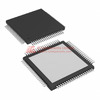
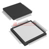
Key advantages include its LVDS parallel data interface, which facilitates high-speed data transmission, and its flexible reference type supporting both external and internal references. The compact 48-VQFN (7x7) package enables dense circuit board integration, making it suitable for space-constrained electronic systems.

Potential equivalent or alternative models in the Texas Instruments portfolio include the ADS5445, ADS5540, and ADS5541, which offer similar performance characteristics with slight variations in sampling rates and bit resolutions.

Typical application areas encompass telecommunications infrastructure, medical imaging equipment, high-speed data acquisition systems, scientific instrumentation, radar signal processing, and advanced test and measurement equipment. The device's robust design, coupled with its lead-free RoHS compliance, positions it as a versatile solution for cutting-edge electronic engineering challenges.

ADS5546IRGZT Key Technical Attributes

14 Bit Analog to Digital Converter, 1 Input, Pipelined

ADS5546IRGZT Packing Size

48-VQFN packaging, 7x7 size, QFN48 encapsulation, Material - Lead free / RoHS Compliant

ADS5546IRGZT Application

Used in high-speed data acquisition systems, digital oscilloscopes, and communication systems

ADS5546IRGZT Features

The ADS5546IRGZT offers high-performance data conversion with a sampling rate of 190M per second and operates within a temperature range of -40°C to 85°C. It utilizes a pipelined architecture and supports both differential inputs and an internal or external reference voltage. The data interface can handle LVDS - Parallel as well as parallel configurations. Suitable for precise and high-speed applications where rapid and accurate conversion of analog signals to digital data is required.

ADS5546IRGZT Quality and Safety Features

Compliant with RoHS and features Moisture Sensitivity Level (MSL) 3, ensuring reliability and protection against environmental conditions.

ADS5546IRGZT Compatibility

Compatible across various digital systems due to its flexible voltage supplies ranging from 3V to 3.6V both for digital and analog supply lines.

ADS5546IRGZT Datasheet PDF

For complete and authoritative specifications of ADS5546IRGZT, download the datasheet PDF from our website. Ensure to access the most detailed and precise data for optimal utilization.

Quality Distributor

IC-Components is a premium distributor of Luminary Micro / Texas Instruments products. Ensure to source your ADS5546IRGZT through our channels as we guarantee quality and provide comprehensive support. Visit our website to get a quote or to learn more about our services.

Frequently Asked Questions

I need to replace an older ADS5546 in a legacy system. What are the key considerations and potential pitfalls when migrating to the ADS5546IRGZT, especially regarding pin compatibility and analog/digital voltage rails?
When migrating to the ADS5546IRGZT, ensure your existing board layout is compatible with the 48-VQFN (7x7) package. While the ADS5546IRGZT is a direct part number for the ADS5546, verify that your power supply rails are within the 3 V to 3.6 V range for both analog and digital sections. Any voltage mismatch could lead to device malfunction or damage. Pay close attention to the recommended PCB layout guidelines for thermal management and signal integrity, particularly for the LVDS interface, as these can impact the performance of the ADS5546IRGZT.
For a high-speed data acquisition system operating near the ADS5546IRGZT's 190MSPS limit, what are the critical clocking considerations to avoid jitter-induced performance degradation, and how does the internal versus external reference impact this?
Achieving the full 190MSPS sampling rate with the ADS5546IRGZT requires a low-jitter clock source. For critical applications, using an external clock with a high Quality Factor (Q) and ensuring proper termination and impedance matching on the clock input trace is paramount. If using the internal reference, its stability and noise performance will directly affect the overall accuracy. For the highest performance, an external reference is generally preferred, but careful selection and decoupling of that reference source are also critical to minimize its impact on the ADC's performance at maximum speed.
I'm designing a portable instrument requiring low power consumption. Can the ADS5546IRGZT effectively operate at lower sampling rates (e.g., 50MSPS) while maintaining reasonable power efficiency, or is it primarily optimized for its maximum throughput?
While the ADS5546IRGZT is rated for up to 190MSPS, its power consumption will scale with the sampling rate. Operating at lower sampling rates like 50MSPS will indeed reduce power consumption, though it may not be as power-efficient as dedicated lower-speed ADCs. The pipelined architecture of the ADS5546IRGZT inherently has a certain quiescent current. To optimize power, ensure digital supply voltages are minimized within the 3V to 3.6V range and any unused digital outputs are properly managed.
What are the specific challenges and recommended practices for interfacing the LVDS parallel data output of the ADS5546IRGZT with a FPGA that has limited LVDS input channels, and what is the impact of data rate on the required FPGA resources?
Interfacing the ADS5546IRGZT's LVDS parallel output with an FPGA requires careful routing and potentially deserialization. At 190MSPS, the data rate is substantial, and the number of LVDS lanes needs to be accommodated by the FPGA. You'll need to ensure the FPGA has sufficient LVDS input capabilities and high-speed serializers/deserializers if required. Proper termination of the LVDS pairs on the PCB is essential for signal integrity. The data rate will directly influence the clock speed and processing logic required within the FPGA.
In an industrial control system requiring long-term reliability operating at the upper end of the ADS5546IRGZT's -40°C to 85°C temperature range, what are the key factors that could compromise its performance or lifespan, and what mitigation strategies are recommended?
Operating the ADS5546IRGZT at 85°C, especially under continuous high-speed operation, can impact its long-term reliability. Key factors include thermal management; inadequate heat dissipation can lead to accelerated aging. Ensure sufficient airflow and consider heatsinking if thermal simulations indicate high junction temperatures. Also, power supply stability and noise filtering are critical, as ripple can exacerbate analog performance degradation over time at elevated temperatures. Using the device within specifications and ensuring proper grounding are fundamental mitigation strategies.
I'm considering the ADS5546IRGZT for a new design but am concerned about its input type. What are the implications of its single-ended differential input for system design compared to a true differential input, and what are typical driving circuitry requirements?
The ADS5546IRGZT features a differential input structure, indicated by "Input Type: Differential." This means it expects a balanced differential signal, which offers advantages like common-mode noise rejection and wider dynamic range compared to single-ended inputs. However, it necessitates a differential driver circuit, such as a high-speed differential amplifier or transformer, to convert your analog signal into the required differential format. Incorrect driving circuitry can lead to reduced performance, linearity issues, or even device damage for the ADS5546IRGZT.
For a high-frequency RF sampling application, what are the practical limitations of the ADS5546IRGZT's 14-bit resolution and 190MSPS rate when dealing with wide bandwidth signals, and would a device with higher resolution or a different architecture be more suitable in certain scenarios?
The ADS5546IRGZT offers a good balance of resolution (14-bit) and speed (190MSPS) for many RF sampling applications. However, for extremely wide bandwidth signals or applications demanding higher dynamic range, its 14-bit resolution might become a limitation, potentially leading to insufficient quantization noise floor for faint signals in the presence of strong interferers. If capturing signals with very small signal-to-noise ratios (SNR) or very wide spectral content, an ADC with higher resolution (e.g., 16-bit or more) or a specialized RF ADC architecture might be more appropriate.
My current design uses an older ADC. When evaluating a potential replacement like the ADS5546IRGZT, what are the common trade-offs in terms of signal-to-noise ratio (SNR) and effective number of bits (ENOB) compared to similar parts from different manufacturers, and how does the MSL rating affect storage and handling before soldering?
When comparing the ADS5546IRGZT to other ADCs, trade-offs will exist. While the ADS5546IRGZT offers a 190MSPS sampling rate and 14-bit resolution, its SNR and ENOB performance must be evaluated against competing parts at specific input frequencies and signal levels. Datasheet specifications for SNR and ENOB should be reviewed carefully. The Moisture Sensitivity Level (MSL) 3 for the ADS5546IRGZT (168 Hours) indicates it is susceptible to moisture absorption. Proper storage in dry conditions and adherence to recommended baking procedures before soldering are crucial to prevent device damage and ensure reliability.
How does the choice between internal and external reference for the ADS5546IRGZT impact the overall system cost and design complexity, and what are the specific benefits of each in terms of accuracy and stability for different applications?
Using the internal reference of the ADS5546IRGZT simplifies the design and reduces component count and cost. However, the performance of the internal reference is a key factor. For applications demanding the highest accuracy and stability, an external precision voltage reference is typically recommended. This adds cost and complexity (requiring a stable external component and proper decoupling), but it allows for selection of a reference with superior temperature drift and low noise characteristics, which directly benefits the ADC's overall accuracy.
For integration into an embedded system, what are the primary considerations for the parallel data interface configuration of the ADS5546IRGZT, particularly when interfacing with microcontrollers that may have limited parallel I/O pins or slower clock speeds?
The ADS5546IRGZT features a parallel data interface. When interfacing with microcontrollers, consider the number of parallel data pins required, which is directly related to the 14-bit output width and the data rate. If the microcontroller has limited I/O, you might need to implement multiplexing or use a wider bus if available. Additionally, ensure the microcontroller's I/O can reliably sample the data at the desired rate. The LVDS parallel output of the ADS5546IRGZT may require level translation or specific interface chips if the microcontroller's logic levels are not compatible.

Recent Reviews

Leave Comment
Hello, you have not logged in, please log in
User Login

Forgot password?

No account yet? Register now

Tips
Please speak legally
Your email will be hidden
Please complete all required fields ( denoted with* )
Mark
5.0

You May Also Be Interested In:


ADS5546IRGZT

ADS5546IRGZT

Texas Instruments

IC ADC 14BIT PIPELINED 48VQFN

In Stock: 295

SUBMIT RFQ