Choose your country or region.

48-VQFN-Exposed-Pad-RGZ.jpg ImageView larger image
Image may be representation.
See specs for product details.

ADS5545IRGZT

In Stock 294 pcs Reference Price(In US Dollars)
250+
$133.7229
Manufacturer Part Number:
ADS5545IRGZT
Manufacturer / Brand
Texas Instruments
Part of Description:
IC ADC 14BIT PIPELINED 48VQFN
Datasheets:
ADS5545IRGZT(1).pdfADS5545IRGZT(2).pdf
Lead Free Status / RoHS Status:
ROHS3 Compliant
Stock Condition:
New original, 294 pcs Stock Available.
ECAD Model:
Ship From:
Hong Kong
Shipment Way:
DHL/Fedex/TNT/UPS

Inquiry Online

Please complete all required fields with your contact information.Click "SUBMIT REQUEST" we will contact you shortly by email. Or Email us: Info@IC-Components.com
Part Number
Manufacturer
Require Quantity
Target Price(USD)
Company Name
Contact Name
E-mail
Phone
Message
Please enter Verify Code and click "Submit"
Part Number ADS5545IRGZT
Manufacturer / Brand Texas Instruments
Stock Quantity 294 pcs Stock
Category Integrated Circuits (ICs) > Data Acquisition - Analog to Digital Converters (ADC)
Description IC ADC 14BIT PIPELINED 48VQFN
Lead Free Status / RoHS Status: ROHS3 Compliant
RFQ ADS5545IRGZT Datasheets ADS5545IRGZT Details PDF
ADS5545IRGZT Details PDF for KR.pdf
ADS5545IRGZT Details PDF for IT.pdf
ADS5545IRGZT Details PDF for ES.pdf
ADS5545IRGZT Details PDF for DE.pdf
ADS5545IRGZT Details PDF for FR.pdf
Voltage - Supply, Digital 3V ~ 3.6V
Voltage - Supply, Analog 3V ~ 3.6V
Supplier Device Package 48-VQFN (7x7)
Series -
Sampling Rate (Per Second) 170M
Reference Type External, Internal
Ratio - S/H:ADC 1:1
Package / Case 48-VFQFN Exposed Pad
Package Tape & Reel (TR)
Operating Temperature -40°C ~ 85°C
Number of Inputs 1
Number of Bits 14
Number of A/D Converters 1
Mounting Type Surface Mount
Input Type Differential
Features -
Data Interface LVDS - Parallel, Parallel
Configuration S/H-ADC
Base Product Number ADS5545
Architecture Pipelined

Packaging & ESD

Industry-standard static shielding packaging is used for electronic components.Anti-static, light-transparent materials allow easy identification of ICs and PCB assemblies.
The packaging structure provides electrostatic protection based on Faraday cage principles.This helps protect sensitive components from static discharge during handling and transportation.


All products are packed in ESD-safe anti-static packaging. Outer packaging labels include part number, brand, and quantity for clear identification. Goods are inspected prior to shipment to ensure proper condition and authenticity.

ESD protection is maintained throughout packing, handling, and global transportation. Secure packaging provides reliable sealing and resistance during transit. Additional cushioning materials are applied when required to protect sensitive components.

QC(Part Testing by IC Components)Quality Warranty

We can offer worldwide express delivery service, such as DHLor FedEx or TNT or UPS or other forwarder for shipment.

Global Shipment by DHL/FedEx/TNT/UPS

Shipping Fees reference DHL/FedEx
1). You can offer your express delivery account for shipment, ifyou haven’t any express account for shipment, we can offer our account inadvance.
2). Use our account for shipment, Shipment charges(Reference DHL/FedEx, Different Countries has different price.)
Shipment charges: (Reference DHL and FedEX)
Weight(KG): 0.00kg-1.00kg Price(USD$) : USD$60.00
Weight(KG): 1.00kg-2.00kg Price(USD$) : USD$80.00
* The price of cost is reference with DHL/FedEx. The detail charges, please contact us. Different country the express charges are different.


We accept the payment terms: Telegraphic Transfer(T/T), Credit Card, PayPal and Western Union.

PayPal:

PayPal Bank Information:
Company Name : IC COMPONENTS LTD
Paypal ID: PayPal@IC-Components.com

BANK TRANSFAR (Telegraphic Transfer)

Payment For Telegraphic Transfers:
Company Name : IC COMPONENTS LTD Beneficiary Account Number : 549-100669-701
Beneficiary Bank name : Bank of Communications (Hong Kong) Ltd Beneficiary Bank Code : 382 (for local payment)
Beneficiary Bank SWIFT : COMMHKHK
Beneficiary Bank Address : Tsuen Wan Market Street Branch 53 Market Street, Tsuen Wan N.T., Hong Kong

Any inquires or questions, please kindly contact us Email: Info@IC-Components.com


ADS5545IRGZT Product Details:

The ADS5545IRGZT is a high-performance 14-bit analog-to-digital converter (ADC) designed by Texas Instruments, specifically engineered for precision signal conversion in demanding electronic applications. This advanced integrated circuit offers exceptional performance in data acquisition systems, particularly in high-speed, high-resolution signal processing environments.

The converter features a sophisticated pipelined architecture that enables an impressive sampling rate of 170 million samples per second, making it ideal for applications requiring rapid and accurate signal digitization. Its differential input configuration ensures superior noise rejection and signal integrity, which is critical in sensitive measurement and communication systems.

Key technical capabilities include a 14-bit resolution that provides extremely detailed signal representation, with operational stability across a wide temperature range of -40°C to 85°C. The device supports both external and internal reference voltage configurations, offering design flexibility for various system requirements. It operates with a digital and analog supply voltage range of 3V to 3.6V, ensuring compatibility with modern low-power electronic designs.

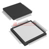
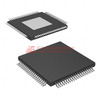
The converter utilizes LVDS (Low-Voltage Differential Signaling) parallel data interface, which enables high-speed, noise-resistant data transmission. Its compact 48-VQFN (7x7) package design allows for efficient board integration and minimizes overall system footprint.

Primary application areas include telecommunications infrastructure, high-speed data acquisition systems, test and measurement equipment, software-defined radio, and advanced signal processing platforms. The device's robust performance makes it particularly suitable for applications demanding precision signal conversion with minimal distortion.

Equivalent or alternative models in the Texas Instruments product lineup include the ADS5544, ADS5546, and ADS5547, which offer similar architectural principles with variations in sampling rates, resolution, and specific feature sets.

The product is lead-free and RoHS compliant, meeting contemporary environmental and regulatory standards for electronic components. Its moisture sensitivity level (MSL) of 3 indicates specific handling and storage requirements to maintain optimal performance.

This ADC represents a sophisticated solution for engineers seeking high-performance signal digitization with exceptional speed, accuracy, and reliability across diverse electronic design challenges.

ADS5545IRGZT Key Technical Attributes

14 Bit

170M Sampling Rate

Pipelined Architecture

ADS5545IRGZT Packing Size

Package Type: 48-VQFN (7x7)

Material: Plastic Encapsulate QFN48

Pins: 48

Thermal Characteristics: Operating Temperature -40°C to 85°C

Electrical Properties: 3 V ~ 3.6 V for both Analog and Digital Supply Voltage

ADS5545IRGZT Application

This device is suited for high-speed signal processing applications such as imaging systems, digital data acquisition, and communication systems.

ADS5545IRGZT Features

The ADS5545IRGZT offers a high-speed 14-bit analog to digital conversion with a maximum sampling rate of 170 million samples per second. Featuring a pipelined architecture, it can perform high-level and precise data conversion from analog to digital. It supports both differential input types and dual voltage supply for analog and digital circuitry, complementing various system design requirements. With the ability to use either external or internal reference types, versatility in integration into existing design frameworks is greatly enhanced.

ADS5545IRGZT Quality and Safety Features

The ADS5545IRGZT is designed under strict compliance with RoHS standards providing lead-free assurance for environmental safety. It features a Moisture Sensitivity Level (MSL) of 3, ensuring durability and reliability in high-moisture conditions up to 168 hours.

ADS5545IRGZT Compatibility

Featuring LVDS and parallel data interfaces, the ADS5545IRGZT can integrate easily with most of the existing digital systems, offering flexibility in design and application.

ADS5545IRGZT Datasheet PDF

Our website provides the most authoritative datasheet for the ADS5545IRGZT. For detailed specifications and operational guidance, we recommend downloading it directly from the current page to ensure you receive the most accurate and up-to-date information.

Quality Distributor

IC-Components stands as a premium distributor of Texas Instruments products, providing trusted and effective service. As an authorized dealer, we guarantee the best deals and the originality of your components. Get your quote today on our website and ensure you're picking the best in market components for your needs.

Frequently Asked Questions

When designing a high-speed data acquisition system with the ADS5545IRGZT, what are the critical considerations for its differential analog input impedance to avoid signal reflections and maintain signal integrity, especially when interfacing with external analog front-end circuits like filters or amplifiers?
The ADS5545IRGZT features a differential analog input with a nominal input impedance. To ensure optimal signal transfer and minimize reflections, it is crucial to match the source impedance of the analog front-end circuit to the differential input impedance of the ADS5545IRGZT. This often involves using appropriate termination resistors, typically placed close to the ADC's input pins, and carefully designing the impedance of the preceding filter or amplifier stages. Referencing the ADS5545IRGZT datasheet for specific impedance values and recommended termination schemes is essential for a successful design.
I'm migrating from an older 12-bit ADC to the ADS5545IRGZT for improved resolution. What are the key challenges and potential design modifications needed when replacing a single-ended input ADC with the differential input ADS5545IRGZT in an existing PCB layout, considering signal routing and common-mode voltage?
Transitioning to the differential input ADS5545IRGZT from a single-ended ADC requires careful PCB layout modifications. Differential signals are more robust against noise, but require dedicated routing for both positive and negative signal paths to maintain symmetry and minimize skew. You'll need to consider a differential driver for the input signal and implement proper termination for both signals at the ADS5545IRGZT. Furthermore, ensure the analog supply voltage range (3V to 3.6V for the ADS5545IRGZT) is compatible with your existing power regulation.
What are the implications of using an external reference voltage versus the internal reference for the ADS5545IRGZT in terms of accuracy, stability, and potential noise issues in a demanding industrial application operating near its -40°C lower limit?
For applications demanding the highest accuracy and stability, especially in an industrial environment with wide temperature variations, using an external, high-precision voltage reference is generally recommended for the ADS5545IRGZT. While the internal reference offers convenience, its temperature coefficient and susceptibility to internal noise might not meet stringent requirements. An external reference should be carefully selected for its own stability, low noise, and appropriate voltage output to drive the ADS5545IRGZT's reference input effectively.
Considering the 170MSPS sampling rate of the ADS5545IRGZT, what are the critical timing constraints and clocking jitter requirements for the system clock input to ensure the full 14-bit resolution is achieved without significant performance degradation?
Achieving the full 170MSPS sampling rate and 14-bit resolution with the ADS5545IRGZT necessitates a low-jitter clock source. Clock jitter directly translates to effective resolution loss (ENOB reduction). The ADS5545IRGZT datasheet will specify the maximum allowable clock jitter for a given sampling rate and desired ENOB. It's crucial to use a well-designed clocking scheme, potentially employing crystal oscillators with appropriate buffering and minimizing trace length and impedance mismatches in the clock path.
If a component failure occurs requiring replacement of the ADS5545IRGZT, what are the primary differences and potential design challenges when considering an alternative 14-bit, ~170MSPS ADC from a different manufacturer, such as a TI model with a similar datasheet but potentially different pinouts or register maps?
Replacing the ADS5545IRGZT with a functionally similar ADC from another manufacturer, even one with comparable specifications, will likely involve significant design effort. Key differences to scrutinize include pinout compatibility (which can mandate PCB redesign), register maps for configuration and control (requiring firmware updates), power supply requirements, and potential differences in analog input characteristics and digital interface signaling levels. Thorough re-validation of the entire analog front-end and digital interface is essential.
What are the common failure modes or reliability concerns associated with the ADS5545IRGZT when operating continuously for extended periods in an environment with fluctuating temperatures within its -40°C to 85°C range, and what design practices can mitigate these?
In extended industrial operation for the ADS5545IRGZT, reliability concerns often revolve around thermal management and component aging. While the device is rated for -40°C to 85°C, continuous operation at the upper end of this range can accelerate aging. Proper PCB thermal design, including adequate copper planes, vias for heat dissipation, and potentially heatsinks if the power dissipation is significant, is vital. Additionally, ensuring stable power supply voltages and using high-quality passive components in the surrounding circuitry will contribute to long-term reliability of the ADS5545IRGZT.
For a compact embedded system requiring a 14-bit ADC with a high sampling rate, what are the trade-offs of using the 48-VQFN (7x7) package of the ADS5545IRGZT concerning thermal performance and ease of assembly compared to a larger package or a different encapsulation type?
The 48-VQFN (7x7) package for the ADS5545IRGZT offers a compact footprint, which is advantageous for space-constrained designs. However, smaller packages generally have lower thermal resistance, meaning heat dissipation is more challenging. Careful PCB layout and potentially thermal vias are crucial for managing heat generated by the ADS5545IRGZT. For very high-power applications or where thermal management is severely limited, a larger package with better thermal properties might be considered, though this would impact board space.
How does the choice between the internal and external reference for the ADS5545IRGZT impact the overall power consumption of the system, and are there specific scenarios where the internal reference might be preferred from a power-saving perspective despite potential accuracy trade-offs?
Using the internal reference of the ADS5545IRGZT generally consumes less power than an external precision voltage reference. The internal reference is integrated and optimized for the device. If the application's accuracy requirements are less stringent or if minimizing power consumption is a primary design goal (e.g., for battery-powered devices), the internal reference of the ADS5545IRGZT might be a viable option. However, for applications demanding the highest signal-to-noise ratio (SNR) and linearity, the added power cost of an external reference is often justified.
In an embedded system where the ADS5545IRGZT is clocked by a distributed clock network, what is the expected impact of clock skew between the ADC clock and the digital data interface clock on data capture accuracy, and how can this be minimized when using the LVDS parallel interface?
Clock skew between the ADC sampling clock and the digital data capture clock for the ADS5545IRGZT's LVDS parallel interface can lead to incorrect data capture. This is because the LVDS interface requires precise timing alignment for reliable data transfer. To minimize skew, it's essential to ensure that the clock paths for both the ADC clock and the digital interface clock are of equal length and impedance on the PCB. Careful routing strategies, including delay compensation techniques, are recommended. The datasheet for the ADS5545IRGZT will provide specific timing diagrams and setup/hold time requirements that must be met.
When considering the ADS5545IRGZT for an application that requires a data acquisition rate of less than 100MSPS, are there any power-saving modes or configuration options that can be utilized to reduce power consumption without significantly compromising performance at the lower sampling frequency?
The ADS5545IRGZT may offer power-down or standby modes that can be activated when the full 170MSPS sampling rate is not required. Consult the ADS5545IRGZT datasheet for specific details on such features. By disabling certain internal blocks or reducing clock speeds, power consumption can be significantly lowered. Careful analysis of the datasheet's power consumption figures at different operating frequencies and modes is necessary to determine the optimal configuration for your reduced sampling rate requirement.

Recent Reviews

Leave Comment
Hello, you have not logged in, please log in
User Login

Forgot password?

No account yet? Register now

Tips
Please speak legally
Your email will be hidden
Please complete all required fields ( denoted with* )
Mark
5.0

You May Also Be Interested In:


ADS5545IRGZT

ADS5545IRGZT

Texas Instruments

IC ADC 14BIT PIPELINED 48VQFN

In Stock: 294

SUBMIT RFQ