Choose your country or region.

8-VDFN.jpg ImageView larger image
Image may be representation.
See specs for product details.

UCC27211DRMR

In Stock 25400 pcs Reference Price(In US Dollars)
1+
$2.6669
10+
$2.2601
30+
$2.0183
100+
$1.7736
500+
$1.6607
1000+
$1.6101
Manufacturer Part Number:
UCC27211DRMR
Manufacturer / Brand
Texas Instruments
Part of Description:
IC GATE DRVR HALF-BRIDGE 8VSON
Datasheets:
UCC27211DRMR(1).pdfUCC27211DRMR(2).pdfUCC27211DRMR(3).pdf
Lead Free Status / RoHS Status:
ROHS3 Compliant
Stock Condition:
New original, 25400 pcs Stock Available.
ECAD Model:
Ship From:
Hong Kong
Shipment Way:
DHL/Fedex/TNT/UPS

Inquiry Online

Please complete all required fields with your contact information.Click "SUBMIT REQUEST" we will contact you shortly by email. Or Email us: Info@IC-Components.com
Part Number
Manufacturer
Require Quantity
Target Price(USD)
Company Name
Contact Name
E-mail
Phone
Message
Please enter Verify Code and click "Submit"
Part Number UCC27211DRMR
Manufacturer / Brand Texas Instruments
Stock Quantity 25400 pcs Stock
Category Integrated Circuits (ICs) > Power Management (PMIC) - Gate Drivers
Description IC GATE DRVR HALF-BRIDGE 8VSON
Lead Free Status / RoHS Status: ROHS3 Compliant
RFQ UCC27211DRMR Datasheets UCC27211DRMR Details PDF
UCC27211DRMR Details PDF for FR.pdf
UCC27211DRMR Details PDF for KR.pdf
UCC27211DRMR Details PDF for IT.pdf
UCC27211DRMR Details PDF for DE.pdf
UCC27211DRMR Details PDF for ES.pdf
Voltage - Supply 8V ~ 17V
Supplier Device Package 8-VSON (4x4)
Series -
Rise / Fall Time (Typ) 7.2ns, 5.5ns
Package / Case 8-VDFN Exposed Pad
Package Tape & Reel (TR)
Operating Temperature -40°C ~ 140°C (TJ)
Number of Drivers 2
Mounting Type Surface Mount
Logic Voltage - VIL, VIH 1.3V, 2.7V
Input Type Non-Inverting
High Side Voltage - Max (Bootstrap) 120 V
Gate Type N-Channel MOSFET
Driven Configuration Half-Bridge
Current - Peak Output (Source, Sink) 4A, 4A
Channel Type Independent
Base Product Number UCC27211

Packaging & ESD

Industry-standard static shielding packaging is used for electronic components.Anti-static, light-transparent materials allow easy identification of ICs and PCB assemblies.
The packaging structure provides electrostatic protection based on Faraday cage principles.This helps protect sensitive components from static discharge during handling and transportation.


All products are packed in ESD-safe anti-static packaging. Outer packaging labels include part number, brand, and quantity for clear identification. Goods are inspected prior to shipment to ensure proper condition and authenticity.

ESD protection is maintained throughout packing, handling, and global transportation. Secure packaging provides reliable sealing and resistance during transit. Additional cushioning materials are applied when required to protect sensitive components.

QC(Part Testing by IC Components)Quality Warranty

We can offer worldwide express delivery service, such as DHLor FedEx or TNT or UPS or other forwarder for shipment.

Global Shipment by DHL/FedEx/TNT/UPS

Shipping Fees reference DHL/FedEx
1). You can offer your express delivery account for shipment, ifyou haven’t any express account for shipment, we can offer our account inadvance.
2). Use our account for shipment, Shipment charges(Reference DHL/FedEx, Different Countries has different price.)
Shipment charges: (Reference DHL and FedEX)
Weight(KG): 0.00kg-1.00kg Price(USD$) : USD$60.00
Weight(KG): 1.00kg-2.00kg Price(USD$) : USD$80.00
* The price of cost is reference with DHL/FedEx. The detail charges, please contact us. Different country the express charges are different.


We accept the payment terms: Telegraphic Transfer(T/T), Credit Card, PayPal and Western Union.

PayPal:

PayPal Bank Information:
Company Name : IC COMPONENTS LTD
Paypal ID: PayPal@IC-Components.com

BANK TRANSFAR (Telegraphic Transfer)

Payment For Telegraphic Transfers:
Company Name : IC COMPONENTS LTD Beneficiary Account Number : 549-100669-701
Beneficiary Bank name : Bank of Communications (Hong Kong) Ltd Beneficiary Bank Code : 382 (for local payment)
Beneficiary Bank SWIFT : COMMHKHK
Beneficiary Bank Address : Tsuen Wan Market Street Branch 53 Market Street, Tsuen Wan N.T., Hong Kong

Any inquires or questions, please kindly contact us Email: Info@IC-Components.com


UCC27211DRMR Product Details:

The UCC27211DRMR is a high-performance half-bridge gate driver integrated circuit designed by Texas Instruments, specifically engineered to provide robust and efficient control for N-Channel MOSFET switching applications across a wide range of electronic systems. This advanced device addresses critical design challenges in power management and motor control circuits by offering precise and rapid gate driving capabilities.

The gate driver operates across an extended temperature range of -40°C to 140°C, making it suitable for demanding industrial and automotive environments. It features an innovative non-inverting input configuration with independent channel control, enabling synchronized and precise MOSFET switching with exceptionally fast rise and fall times of 7.2ns and 5.5ns respectively.

Designed for versatility, the UCC27211DRMR supports a supply voltage range of 8V to 17V and delivers impressive peak output currents of 4A for both sourcing and sinking. Its high-side voltage capability reaches up to 120V during bootstrap operations, providing significant headroom for complex power conversion and switching applications.

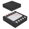
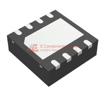
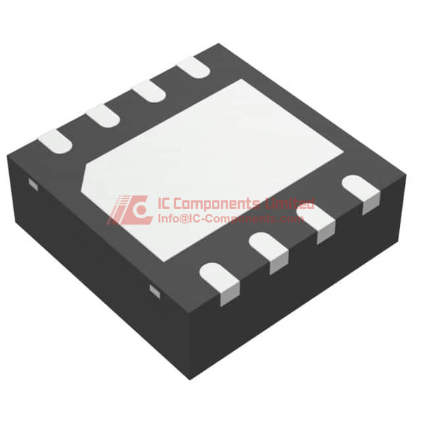
The device is packaged in a compact 8-VSON (4x4) surface-mount format, facilitating easy integration into space-constrained electronic designs. Its lead-free and RoHS-compliant construction ensures environmental responsibility and adherence to modern manufacturing standards.

Primary advantages include low propagation delay, robust protection against electrical noise, and the ability to drive high-performance N-Channel MOSFETs efficiently. Typical application areas encompass motor drives, power inverters, solar inverters, uninterruptible power supplies, and various industrial power conversion systems.

Equivalent or alternative models that offer similar functionality include the UCC27210, UCC27212, and LM5107, which provide comparable half-bridge gate driving capabilities with slight variations in specifications and performance characteristics.

The UCC27211DRMR's comprehensive feature set, reliability, and compact design make it an excellent choice for engineers seeking a high-performance gate driver solution across diverse power electronics applications.

UCC27211DRMR Key Technical Attributes

Manufacturer Part Number: UCC27211DRMR

Manufacturer: Luminary Micro / Texas Instruments

Detail: Half-Bridge Gate Driver IC Non-Inverting 8-VSON (4x4)

UCC27211DRMR Packing Size

Type: Tape & Reel (TR)

Material: VSON-8

Size: 8-VSON (4x4)

Pin Configuration: 8-VDFN Exposed Pad

Thermal Characteristics: Operating Temperature -40°C ~ 140°C (TJ)

Electrical Properties: Voltage - Supply: 8 V ~ 17 V

UCC27211DRMR Application

The UCC27211DRMR is utilized primarily in high-efficiency, high-density power applications including DC/DC converters, motor control, and power supplies.

UCC27211DRMR Features

The UCC27211DRMR is a Half-Bridge Gate Driver IC featuring independent channel operation with a non-inverting configuration. It supports a supply voltage range of 8 V to 17 V and delivers peak output currents of 4A for both sourcing and sinking. Incorporated gate drivers are specifically designed to drive N-Channel MOSFETs in a half-bridge configuration. It boasts fast rise and fall times of 7.2ns and 5.5ns respectively. High Side Voltage can go up to 120V, and logic voltage levels are set at 1.3V for VIL and 2.7V for VIH.

UCC27211DRMR Quality and Safety Features

The UCC27211DRMR features a Moisture Sensitivity Level (MSL) of 1, indicating unlimited floor life under standard conditions. It is also RoHS Compliant ensuring it meets the latest environmental standards concerning hazardous substances.

UCC27211DRMR Compatibility

This gate driver IC is compatible with any application requiring the driving of N-Channel MOSFET configurations in a half-bridge setup. It operates efficiently across a broad temperature range from -40°C to 140°C, suitable for harsh environments.

UCC27211DRMR Datasheet PDF

Our website provides the most authoritative and comprehensive datasheet for the UCC27211DRMR. Ensure you download it from the current page for complete product specifications and application guidance.

Quality Distributor

IC-Components is a celebrated distributor of products from Luminary Micro / Texas Instruments. We guarantee premium service and authentic components. For expert advice and competitive quotes, make sure to contact us through our website today.

Frequently Asked Questions

Can the UCC27211DRMR be used in a 48V industrial motor drive application with high-side switching above 60V, and what bootstrap component selection considerations apply?
Yes, the UCC27211DRMR is suitable for 48V motor drive applications, as its high-side bootstrap circuitry supports up to 120V. However, when operating above 60V, careful selection of the bootstrap diode and capacitor is critical to ensure reliable charging under high dV/dt conditions. Use a fast-recovery or Schottky diode with a reverse voltage rating exceeding the bus voltage by at least 20%, and select a low-ESR ceramic capacitor (typically 100nF to 1µF) rated for the full bootstrap voltage. Ensure the bootstrap capacitor recharge time is sufficient during low-duty-cycle operation to prevent undervoltage lockout on the high-side driver.
What are the key differences between the UCC27211DRMR and the UCC27212DRMR, and can they be used interchangeably in a half-bridge design?
The UCC27211DRMR and UCC27212DRMR differ primarily in input logic compatibility and propagation delay matching. The UCC27211DRMR accepts TTL-level inputs (VIL = 1.3V, VIH = 2.7V), making it ideal for direct interfacing with 3.3V or 5V logic controllers, while the UCC27212DRMR uses CMOS thresholds. Additionally, the UCC27212 has tighter propagation delay matching between channels. They are not directly interchangeable without verifying logic compatibility and timing requirements in your control circuit. Substituting one for the other may require level-shifting or firmware adjustments, especially in high-frequency or dead-time-sensitive applications.
How does the exposed pad on the 8-VSON (4x4) package of the UCC27211DRMR affect PCB layout and thermal performance in high-current switching applications?
The exposed thermal pad on the UCC27211DRMR must be soldered directly to a grounded copper pour on the PCB to ensure both electrical grounding and effective heat dissipation. For high-current or high-frequency switching, connect the pad to a multi-via array (e.g., 4–9 vias) leading to an internal or bottom-layer ground plane. This reduces thermal resistance and prevents localized heating, which could degrade reliability. Poor thermal management may lead to premature failure, especially when operating near the 140°C junction temperature limit. Always follow TI’s recommended land pattern and thermal enhancement guidelines in the datasheet.
Is the UCC27211DRMR suitable for replacing a discrete gate driver solution in a 100W synchronous buck converter, and what integration benefits does it offer?
Yes, the UCC27211DRMR is an excellent replacement for discrete gate driver circuits in a 100W synchronous buck converter. It integrates both high-side and low-side N-channel MOSFET drivers with matched propagation delays (typically 7.2ns rise, 5.5ns fall), reducing timing skew and improving efficiency. The integrated bootstrap diode and under-voltage lockout (UVLO) simplify design, minimize component count, and enhance reliability. Compared to discrete solutions, it reduces PCB footprint, minimizes parasitic inductance, and ensures consistent performance across temperature and manufacturing variations.
What input signal integrity issues should be considered when driving the UCC27211DRMR from a microcontroller operating at 3.3V logic levels?
The UCC27211DRMR’s input logic thresholds (VIL = 1.3V, VIH = 2.7V) are compatible with 3.3V CMOS outputs, but signal integrity must be maintained to avoid false triggering. Ensure clean, fast-edged PWM signals with minimal ringing or overshoot, especially in noisy switching environments. Use series termination resistors (e.g., 22–100Ω) near the driver input to dampen reflections, and keep input traces short and away from high di/dt loops. Avoid long, unterminated traces that could act as antennas, as electromagnetic interference may couple into the input and cause unintended switching.
Can the UCC27211DRMR operate reliably in an automotive under-hood environment with ambient temperatures reaching 125°C?
Yes, the UCC27211DRMR is rated for a junction temperature (TJ) of up to 140°C and can operate reliably in automotive under-hood environments where ambient temperatures reach 125°C, provided proper thermal design is implemented. Ensure the PCB layout maximizes heat dissipation through the exposed pad and that airflow or conduction cooling is sufficient to keep TJ within limits. Derating input frequency or duty cycle may be necessary under extreme thermal conditions. Additionally, verify that all surrounding components (e.g., bootstrap capacitors, MOSFETs) are also rated for the same temperature range to ensure system-level reliability.
What dead time management strategies are recommended when using the UCC27211DRMR in a half-bridge configuration to prevent shoot-through?
The UCC27211DRMR does not include built-in dead time control, so dead time must be managed externally by the controller (e.g., MCU or PWM IC). Implement a minimum dead time of 20–50ns in firmware or hardware to account for MOSFET turn-off delay and driver propagation mismatch. Use the UCC27211DRMR’s fast rise/fall times (7.2ns/5.5ns) to your advantage by minimizing unnecessary dead time, which improves efficiency. Monitor switching waveforms with an oscilloscope during prototype testing to verify no cross-conduction occurs, especially under light load or transient conditions.
Are there any known compatibility issues when replacing an older UCC27201 with the UCC27211DRMR in an existing half-bridge design?
The UCC27211DRMR can generally replace the UCC27201, but key differences must be addressed: the UCC27211DRMR has lower input thresholds (TTL-compatible), faster switching speeds, and a smaller 8-VSON package. Verify that your controller’s output logic levels meet the UCC27211DRMR’s VIH/VIL requirements. Also, the reduced propagation delay may require adjustment of dead time settings in the control algorithm. Additionally, the UCC27211DRMR’s exposed pad requires a different PCB footprint, so layout modifications are necessary. Always revalidate thermal performance and switching behavior after substitution.
What is the maximum allowable switching frequency for the UCC27211DRMR in a 48V-to-12V DC-DC converter without exceeding thermal limits?
The maximum switching frequency for the UCC27211DRMR depends on load current, gate charge of the driven MOSFETs, and thermal design. For typical 48V-to-12V converters using 100V N-channel MOSFETs with total gate charge (Qg) of 20–40nC, the UCC27211DRMR can reliably operate up to 500kHz with proper heat sinking. At higher frequencies (e.g., 1MHz), power dissipation in the driver increases due to switching losses; calculate Pd = (Qg × VDRV × fSW) + (ICC × VDD) and ensure TJ remains below 140°C. Use thermal simulation or empirical testing to validate performance in your specific application.
How should the UCC27211DRMR be configured for use in a non-inverting half-bridge topology with complementary PWM inputs?
In a non-inverting half-bridge configuration, connect the PWM signal directly to the HI (high-side) input and its inverted version to the LI (low-side) input of the UCC27211DRMR. Ensure both signals are synchronized and include dead time to prevent shoot-through. The UCC27211DRMR’s non-inverting outputs will drive the high-side and low-side MOSFET gates with the same polarity as the inputs. Use a logic gate or controller with complementary output capability, and verify that the bootstrap capacitor is adequately charged during each switching cycle, especially at low duty cycles. Always decouple the VDD pin with a 1µF ceramic capacitor placed close to the IC.

Recent Reviews

Leave Comment
Hello, you have not logged in, please log in
User Login

Forgot password?

No account yet? Register now

Tips
Please speak legally
Your email will be hidden
Please complete all required fields ( denoted with* )
Mark
5.0

You May Also Be Interested In:


UCC27211DRMR

UCC27211DRMR

Texas Instruments

IC GATE DRVR HALF-BRIDGE 8VSON

In Stock: 25400

SUBMIT RFQ