Choose your country or region.

TC74HC07AF.jpg ImageTC74HC07AF.jpg ImageView larger imageView larger image
Image may be representation.
See specs for product details.

TC74HC07AF

In Stock 40770 pcs Reference Price(In US Dollars)
1+
$0.5829
Manufacturer Part Number:
TC74HC07AF
Manufacturer / Brand
TOSHIBA
Part of Description:
TC74HC07AF TOSHIBA SOP
Datasheets:
Lead Free Status / RoHS Status:
RoHS Compliant
Stock Condition:
New original, 40770 pcs Stock Available.
ECAD Model:
Ship From:
Hong Kong
Shipment Way:
DHL/Fedex/TNT/UPS

Inquiry Online

Please complete all required fields with your contact information.Click "SUBMIT REQUEST" we will contact you shortly by email. Or Email us: Info@IC-Components.com
Part Number
Manufacturer
Require Quantity
Target Price(USD)
Company Name
Contact Name
E-mail
Phone
Message
Please enter Verify Code and click "Submit"
Part Number TC74HC07AF
Manufacturer / Brand TOSHIBA
Stock Quantity 40770 pcs Stock
Category Integrated Circuits (ICs) > Specialized ICs
Description TC74HC07AF TOSHIBA SOP
Lead Free Status / RoHS Status: RoHS Compliant
RFQ TC74HC07AF Datasheets TC74HC07AF Details PDF
TC74HC07AF Details PDF for FR.pdf
TC74HC07AF Details PDF for KR.pdf
TC74HC07AF Details PDF for IT.pdf
TC74HC07AF Details PDF for ES.pdf
TC74HC07AF Details PDF for DE.pdf
Package SOP
Condition New Original Stock
Warranty 100% Perfect Functions
Lead Time 2-3days after payment.
Payment Credit Card / PayPal / Telegraphic Transfer (T/T) / Western Union
Shipping by DHL / Fedex / UPS / TNT
Port HongKong
RFQ Email Info@IC-Components.com

Packaging & ESD

Industry-standard static shielding packaging is used for electronic components.Anti-static, light-transparent materials allow easy identification of ICs and PCB assemblies.
The packaging structure provides electrostatic protection based on Faraday cage principles.This helps protect sensitive components from static discharge during handling and transportation.


All products are packed in ESD-safe anti-static packaging. Outer packaging labels include part number, brand, and quantity for clear identification. Goods are inspected prior to shipment to ensure proper condition and authenticity.

ESD protection is maintained throughout packing, handling, and global transportation. Secure packaging provides reliable sealing and resistance during transit. Additional cushioning materials are applied when required to protect sensitive components.

QC(Part Testing by IC Components)Quality Warranty

We can offer worldwide express delivery service, such as DHLor FedEx or TNT or UPS or other forwarder for shipment.

Global Shipment by DHL/FedEx/TNT/UPS

Shipping Fees reference DHL/FedEx
1). You can offer your express delivery account for shipment, ifyou haven’t any express account for shipment, we can offer our account inadvance.
2). Use our account for shipment, Shipment charges(Reference DHL/FedEx, Different Countries has different price.)
Shipment charges: (Reference DHL and FedEX)
Weight(KG): 0.00kg-1.00kg Price(USD$) : USD$60.00
Weight(KG): 1.00kg-2.00kg Price(USD$) : USD$80.00
* The price of cost is reference with DHL/FedEx. The detail charges, please contact us. Different country the express charges are different.


We accept the payment terms: Telegraphic Transfer(T/T), Credit Card, PayPal and Western Union.

PayPal:

PayPal Bank Information:
Company Name : IC COMPONENTS LTD
Paypal ID: PayPal@IC-Components.com

BANK TRANSFAR (Telegraphic Transfer)

Payment For Telegraphic Transfers:
Company Name : IC COMPONENTS LTD Beneficiary Account Number : 549-100669-701
Beneficiary Bank name : Bank of Communications (Hong Kong) Ltd Beneficiary Bank Code : 382 (for local payment)
Beneficiary Bank SWIFT : COMMHKHK
Beneficiary Bank Address : Tsuen Wan Market Street Branch 53 Market Street, Tsuen Wan N.T., Hong Kong

Any inquires or questions, please kindly contact us Email: Info@IC-Components.com


TC74HC07AF Product Details:

The TC74HC07AF is a specialized integrated circuit (IC) manufactured by Toshiba Electronic Devices and Storage Corporation, designed to provide robust buffering and signal conditioning capabilities in electronic systems. This hex buffer/driver IC is part of the 74HC series, which offers high-speed, low-power performance for various electronic applications.

The device features six independent buffer stages with open-collector outputs, making it ideal for applications requiring signal inversion, driving high-impedance loads, or creating flexible logic interfaces. Its SOP (Small Outline Package) encapsulation ensures compact design and efficient PCB integration, addressing space constraints in modern electronic devices.

Key specifications include high-speed switching capabilities, low power consumption, and compatibility with standard logic families. The circuit provides excellent noise immunity and can operate across a wide voltage range, making it suitable for diverse electronic design requirements. Its open-collector architecture allows for wire-OR implementation and easy interfacing with multiple logic systems.

Primary advantages include its versatility in signal routing, buffer amplification, and logic-level translation. The TC74HC07AF is particularly well-suited for industrial control systems, telecommunications equipment, computer peripherals, and consumer electronics where reliable signal handling is critical.

Equivalent or alternative models in the same family include:

- MC74HC07ADR2G

- SN74HC07NSR

- CD74HC07M96

- 74HC07D,653

The component supports a wide range of electronic design applications, offering engineers a reliable and efficient solution for signal buffering and driver requirements in compact electronic systems.
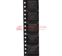
TC74HC07AF Image
TC74HC07AF (1)

TC74HC07AF Key Technical Attributes

Manufacturer Part Number TC74HC07AF

Manufacturer Toshiba Electronic Devices and Storage Corporation (TAEC)

TC74HC07AF Packing Size

Type SOP (Small Outline Package)

Material High-quality molded plastic with excellent durability

Size Standard SOP dimensions with 674 encapsulation code

Pin Configuration 14 pins arranged in dual in-line format for efficient circuit integration

Thermal Characteristics Low power dissipation with enhanced heat resistance suitable for industrial applications

Electrical Properties High noise immunity, operating voltage range typically from 2V to 6V, and standard CMOS logic levels

TC74HC07AF Application

The TC74HC07AF is widely used in digital logic interface circuits requiring open-drain outputs. Ideal for driving LED displays, relay circuits, and bus interface applications, it suits industrial automation, signal buffering, and level shifting tasks. Its high noise immunity makes it suitable for automotive and telecommunications equipment.

TC74HC07AF Features

This device incorporates six independent open-drain buffer gates with high voltage tolerance and low static power consumption. The open-drain outputs allow for wired-AND configurations and multi-point bus connections. It features wide operating voltage ranges, rapid switching speeds, and output drive capabilities compatible with TTL levels. The built-in protection against electrostatic discharge (ESD) ensures operational stability and longevity. Its high impedance inputs minimize loading effects on preceding stages, contributing to enhanced signal integrity in complex circuits.
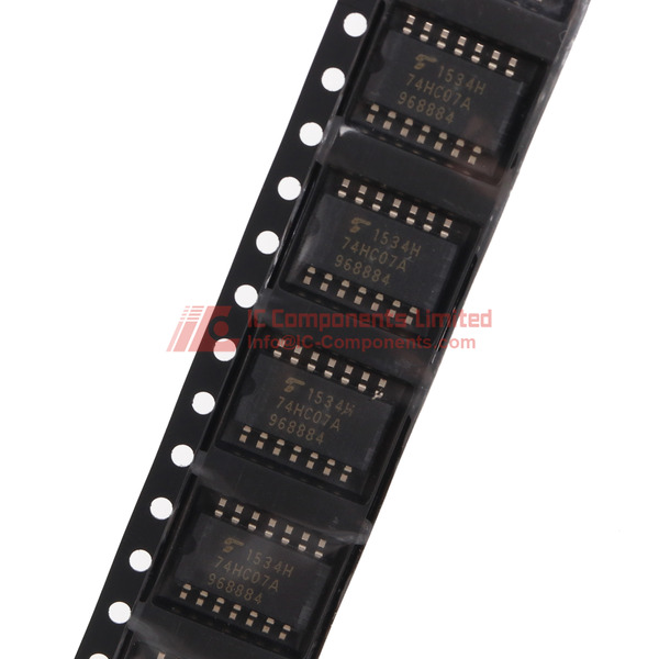
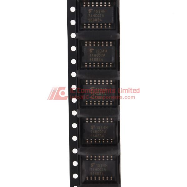
TC74HC07AF Image
TC74HC07AF (2)

TC74HC07AF Quality and Safety Features

Manufactured under stringent Toshiba quality control standards, the TC74HC07AF ensures consistent performance and reliability. The IC complies with international safety and environmental standards, including RoHS directives for hazardous substance control. Its robust construction provides high tolerance to temperature fluctuations and electromagnetic interference, securing safe operation in harsh environments. Continuous reliability testing guarantees long-term stability under extended usage conditions.

TC74HC07AF Compatibility

The TC74HC07AF seamlessly integrates with a wide range of TTL and CMOS logic families, promoting ease of design in mixed-technology systems. Its pin configuration and electrical characteristics align with industry standards, enabling drop-in replacement or upgrade in existing circuit designs. Compatible with standard digital IC sockets and surface-mount assembly processes, it facilitates efficient manufacturing workflows.

TC74HC07AF Datasheet PDF

Our website offers the most authoritative and up-to-date datasheet for the TC74HC07AF, providing comprehensive technical details, application guidelines, and performance graphs. Customers are strongly encouraged to download this datasheet on the current page to ensure accurate design implementation and optimal device utilization.

Quality Distributor

IC-Components is a premium authorized distributor of Toshiba Electronic Devices and Storage Corporation products. We pride ourselves on delivering genuine, high-quality TC74HC07AF ICs backed by exceptional customer service. Visit our website today to request a competitive quote and benefit from our fast shipping and dedicated support tailored to your procurement needs.

Frequently Asked Questions

What are the key design considerations when using the TC74HC07AF in a mixed-voltage system where the input signals are 5V TTL but the output needs to drive a 3.3V CMOS load?
The TC74HC07AF is a hex buffer with open-drain outputs, which makes it suitable for level-shifting applications. However, since it operates with a supply voltage (VCC) range of 2V to 6V, you must ensure VCC is set to 3.3V to match the target logic level. Inputs are 5V-tolerant due to the HC family’s input structure, allowing direct connection to 5V TTL signals without damage. An external pull-up resistor to 3.3V on each output is required to achieve valid high logic levels. Ensure the pull-up value balances rise time and power consumption—typically 1kΩ to 10kΩ depending on bus capacitance and speed requirements.
Can the TC74HC07AF be used as a direct replacement for the 74HCT07 in an existing industrial control board operating at 5V?
While both are hex buffers with open-drain outputs, the TC74HC07AF (HC logic family) has different input threshold characteristics compared to the 74HCT07 (HCT family). The HC family uses CMOS thresholds (~50% of VCC), whereas HCT is designed for TTL-compatible inputs (~1.5V threshold at 5V). If your system relies on marginal TTL signal levels (e.g., 2.0V from older logic), the TC74HC07AF may not reliably recognize low inputs. Verify input signal margins before substitution; otherwise, consider using a true HCT-compatible alternative like the TC74HCT07AF instead.
What are the thermal and reliability implications of operating the TC74HC07AF in a sealed industrial enclosure with ambient temperatures up to 85°C?
The TC74HC07AF is rated for operation from -40°C to +85°C (commercial grade) and housed in an SOP package with limited thermal dissipation. In a sealed enclosure at 85°C ambient, junction temperature can approach or exceed safe limits under continuous high-output loading. Each output can sink up to 25mA (per datasheet), but total package power dissipation must stay below ~500mW. Calculate Pd = VOL × IOL × number of active outputs. If driving multiple lines near max current, consider derating or adding airflow. Long-term reliability may degrade if operated near thermal limits without margin.
Is the TC74HC07AF suitable for driving long PCB traces or cables in a noisy factory environment, and what layout practices should be followed?
The TC74HC07AF’s open-drain outputs can be used for driving longer lines, but signal integrity must be carefully managed. Due to high output impedance when off (only pull-up resistor provides drive), rise times slow significantly with trace/cable capacitance. Use controlled-impedance routing, minimize trace length, and place pull-up resistors close to the load if possible. For cable driving (>30cm), add series termination (22–100Ω) near the TC74HC07AF to reduce reflections. Avoid routing near high-dV/dt signals (e.g., motor drivers) without ground shielding. Consider adding TVS diodes on I/O lines for ESD protection in harsh environments.
How does the TC74HC07AF compare to the SN74LVC07A when migrating a legacy 5V design to a lower-power 3.3V platform?
The TC74HC07AF operates down to 2V VCC and is 5V-input tolerant, making it usable in 3.3V systems with legacy 5V inputs. However, the SN74LVC07A offers lower static power consumption, faster propagation delay (~3.5ns vs ~8ns at 5V), and true 5V-tolerant I/Os with better noise margins at 3.3V. The LVC family also supports partial-power-down protection. If your design prioritizes power efficiency, speed, or integration with modern 3.3V MCUs, the SN74LVC07A is superior. But if you need backward compatibility with existing 5V-only infrastructure and minimal BOM changes, the TC74HC07AF remains a viable, cost-effective option.
What happens if I accidentally connect the TC74HC07AF’s output to a voltage higher than VCC when using open-drain configuration?
The TC74HC07AF’s open-drain outputs are designed to be pulled up to a voltage equal to or less than VCC + 0.5V (per absolute maximum ratings). Connecting an output to a voltage significantly above VCC (e.g., 5V when VCC = 3.3V) risks forward-biasing the ESD protection diodes, causing excessive current flow into the VCC rail. This can damage the device or disrupt other circuitry powered by the same supply. Always ensure the pull-up voltage does not exceed VCC by more than 0.5V. For true voltage translation above VCC, use a dedicated level translator or a device rated for overvoltage-tolerant I/Os like the 74LVC family.
Are there known compatibility issues when replacing a bipolar 74LS07 with the TC74HC07AF in a high-speed digital interface?
Yes—the TC74HC07AF has significantly different input characteristics and propagation delay compared to the 74LS07. The 74LS07 draws higher input current (up to -0.4mA per input) and has TTL thresholds, while the TC74HC07AF has near-zero input current and CMOS thresholds. This mismatch can cause logic errors if driven by weak TTL outputs. Additionally, the TC74HC07AF’s propagation delay (~8ns at 5V) is faster than 74LS07 (~10–15ns), which may affect timing margins in edge-sensitive circuits. Verify signal integrity and fan-out capability; buffering or level-shifting may be needed for reliable operation.
Can the TC74HC07AF be used in a multi-master I²C bus application without additional components?
Yes, the TC74HC07AF’s open-drain outputs make it inherently compatible with I²C bus protocols, which require wired-AND connectivity. However, the TC74HC07AF is not optimized for I²C speeds—its maximum toggle frequency is ~25MHz at 5V, but real-world rise times depend heavily on pull-up resistor values and bus capacitance. For standard-mode I²C (100kHz), it works reliably with appropriate pull-ups (e.g., 4.7kΩ for 400pF bus). For Fast-mode (400kHz) or higher, ensure total bus capacitance stays low and use stronger pull-ups (1kΩ–2.2kΩ). Note that the TC74HC07AF lacks built-in slew rate control or glitch filtering, so noisy environments may require additional filtering.
What is the maximum allowable sink current per output and total package current for the TC74HC07AF under continuous DC operation?
Each output of the TC74HC07AF can sink a maximum of 25mA continuously, and the total supply current (ICC + sum of all IOL) must not exceed 50mA absolute maximum. However, for reliable long-term operation, derate to 20mA per output and keep total package dissipation under 300mW. At 5V VCC and 20mA per output, VOL is typically 0.1V, yielding ~2mW per channel. With all six outputs active, total Pd ≈ 12mW + quiescent power—well within limits—but thermal stacking in dense PCBs or high ambient temperatures necessitates conservative design margins.
Does the SOP package of the TC74HC07AF support automated pick-and-place assembly, and are there any solder reflow or moisture sensitivity concerns?
The TC74HC07AF in SOP (Small Outline Package) is fully compatible with standard SMT pick-and-place equipment and reflow soldering profiles (typically peak 260°C for Pb-free). It is rated MSL (Moisture Sensitivity Level) 1 per JEDEC J-STD-020, meaning it has unlimited floor life under normal storage conditions (≤30°C/60% RH). No baking is required before assembly, reducing handling complexity in high-volume production. Ensure stencil aperture design follows IPC-7351 guidelines for SOP-14 to avoid solder bridging, especially with fine-pitch leads (1.27mm pitch).

Recent Reviews

Leave Comment
Hello, you have not logged in, please log in
User Login

Forgot password?

No account yet? Register now

Tips
Please speak legally
Your email will be hidden
Please complete all required fields ( denoted with* )
Mark
5.0

You May Also Be Interested In:


TC74HC07AF

TC74HC07AF

TOSHIBA

TC74HC07AF TOSHIBA SOP

In Stock: 40770

SUBMIT RFQ