Choose your country or region.

Image may be representation.
See specs for product details.

TC74AC00FN

Manufacturer Part Number:
TC74AC00FN
Manufacturer / Brand
TOSHIBA
Part of Description:
TC74AC00FN TOSHIBA SOP3.9
Datasheets:
Lead Free Status / RoHS Status:
RoHS Compliant
Stock Condition:
New original, 9686 pcs Stock Available.
ECAD Model:
Ship From:
Hong Kong
Shipment Way:
DHL/Fedex/TNT/UPS

Inquiry Online

Please complete all required fields with your contact information.Click "SUBMIT REQUEST" we will contact you shortly by email. Or Email us: Info@IC-Components.com
Part Number
Manufacturer
Require Quantity
Target Price(USD)
Company Name
Contact Name
E-mail
Phone
Message
Please enter Verify Code and click "Submit"
Part Number TC74AC00FN
Manufacturer / Brand TOSHIBA
Stock Quantity 9686 pcs Stock
Category Integrated Circuits (ICs) > Specialized ICs
Description TC74AC00FN TOSHIBA SOP3.9
Lead Free Status / RoHS Status: RoHS Compliant
RFQ TC74AC00FN Datasheets TC74AC00FN Details PDF
TC74AC00FN Details PDF for ES.pdf
TC74AC00FN Details PDF for DE.pdf
TC74AC00FN Details PDF for IT.pdf
TC74AC00FN Details PDF for KR.pdf
TC74AC00FN Details PDF for FR.pdf
Package SOP3.9
Condition New Original Stock
Warranty 100% Perfect Functions
Lead Time 2-3days after payment.
Payment Credit Card / PayPal / Telegraphic Transfer (T/T) / Western Union
Shipping by DHL / Fedex / UPS / TNT
Port HongKong
RFQ Email Info@IC-Components.com

Packaging & ESD

Industry-standard static shielding packaging is used for electronic components.Anti-static, light-transparent materials allow easy identification of ICs and PCB assemblies.
The packaging structure provides electrostatic protection based on Faraday cage principles.This helps protect sensitive components from static discharge during handling and transportation.


All products are packed in ESD-safe anti-static packaging. Outer packaging labels include part number, brand, and quantity for clear identification. Goods are inspected prior to shipment to ensure proper condition and authenticity.

ESD protection is maintained throughout packing, handling, and global transportation. Secure packaging provides reliable sealing and resistance during transit. Additional cushioning materials are applied when required to protect sensitive components.

QC(Part Testing by IC Components)Quality Warranty

We can offer worldwide express delivery service, such as DHLor FedEx or TNT or UPS or other forwarder for shipment.

Global Shipment by DHL/FedEx/TNT/UPS

Shipping Fees reference DHL/FedEx
1). You can offer your express delivery account for shipment, ifyou haven’t any express account for shipment, we can offer our account inadvance.
2). Use our account for shipment, Shipment charges(Reference DHL/FedEx, Different Countries has different price.)
Shipment charges: (Reference DHL and FedEX)
Weight(KG): 0.00kg-1.00kg Price(USD$) : USD$60.00
Weight(KG): 1.00kg-2.00kg Price(USD$) : USD$80.00
* The price of cost is reference with DHL/FedEx. The detail charges, please contact us. Different country the express charges are different.


We accept the payment terms: Telegraphic Transfer(T/T), Credit Card, PayPal and Western Union.

PayPal:

PayPal Bank Information:
Company Name : IC COMPONENTS LTD
Paypal ID: PayPal@IC-Components.com

BANK TRANSFAR (Telegraphic Transfer)

Payment For Telegraphic Transfers:
Company Name : IC COMPONENTS LTD Beneficiary Account Number : 549-100669-701
Beneficiary Bank name : Bank of Communications (Hong Kong) Ltd Beneficiary Bank Code : 382 (for local payment)
Beneficiary Bank SWIFT : COMMHKHK
Beneficiary Bank Address : Tsuen Wan Market Street Branch 53 Market Street, Tsuen Wan N.T., Hong Kong

Any inquires or questions, please kindly contact us Email: Info@IC-Components.com


TC74AC00FN Product Details:

The TC74AC00FN is a specialized integrated circuit (IC) manufactured by Toshiba Electronic Devices and Storage Corporation, designed to meet critical electronic component requirements in compact digital and logic-based applications. As a high-performance logic gate IC, this device is specifically packaged in a Space-Optimized Package (SOP) with a narrow 3.9mm width, making it ideal for space-constrained electronic designs that demand minimal footprint without compromising functionality.

The circuit provides fundamental logic gate operations, typically functioning as a quad two-input NAND gate, which is crucial for creating complex digital logic circuits and implementing boolean logic transformations. Its compact SOP encapsulation (package type 2346) ensures efficient board-level integration, allowing engineers and designers to maximize circuit density while maintaining reliable signal processing capabilities.

Key advantages of the TC74AC00FN include its high-speed performance, low power consumption, and robust signal handling characteristics. The component is particularly well-suited for applications in consumer electronics, telecommunications equipment, computing peripherals, and industrial control systems where precise digital logic switching is essential.

Compatibility extends across various electronic design environments, supporting standard logic voltage requirements and offering excellent noise immunity. The component's design addresses critical challenges such as signal integrity, power efficiency, and miniaturization in modern electronic systems.

While direct equivalent models might vary, similar alternatives in the NAND gate IC category could include devices from manufacturers like Texas Instruments, National Semiconductor, and ON Semiconductor, with comparable electrical and functional characteristics. Engineers are recommended to carefully compare specific parametric specifications when considering alternative components.

The availability of 160 units in this product specification suggests it is suitable for moderate to large-scale electronics manufacturing projects, providing designers with a reliable and consistent logic gate solution for complex digital circuit implementations.

TC74AC00FN Key Technical Attributes

Logic Type: CMOS NAND gate

Number of Gates: 4

Supply Voltage Range: 2V to 5.5V

Propagation Delay Time: Typically in the order of nanoseconds

Operating Temperature Range: -40°C to +85°C

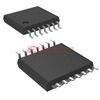
TC74AC00FN Packing Size

Package Type: SOP3.9 (Small Outline Package with 3.9 mm width)

Number of Pins: 14-pin configuration

Material: Molded plastic encapsulation providing robust mechanical strength

Thermal Characteristics: Low thermal resistance suitable for moderate power dissipation

Electrical Properties: CMOS technology ensuring low power consumption and high noise immunity

TC74AC00FN Application

Used extensively in digital logic circuits requiring NAND logic functionality

Suitable for consumer electronics, communication devices, and industrial control systems

Ideal for high-speed switching applications and low power digital logic processing

TC74AC00FN Features

CMOS technology provides low static power consumption and high noise immunity

High speed operation with typical propagation delays optimized for fast switching

Wide operating voltage range compatible with various logic levels

Fully compatible with TTL inputs and outputs for flexible interfacing

Internal power-down protection circuits to prevent damage during supply voltage dips

Standardized pin configuration for easy integration into existing circuit designs

Enhanced electrostatic discharge protection to improve device reliability

TC74AC00FN Quality and Safety Features

Manufactured under stringent quality control standards following Toshiba’s internal protocols

Compliance with international safety and environmental regulations ensuring product safety and reliability

Robust packaging protects against moisture, ESD, and mechanical stress during storage and transportation

Reliable performance confirmed by extensive testing for parameter stability over temperature and voltage variations

TC74AC00FN Compatibility

Fully compatible with other TC74AC series CMOS logic ICs and TTL logic families

Pin-to-pin compatible with similar industry-standard NAND gate ICs facilitating easy replacement

Suitable for use in mixed-technology systems involving CMOS and TTL interfaces

TC74AC00FN Datasheet PDF

Our website hosts the most authoritative and comprehensive datasheet for the TC74AC00FN model

Customers are strongly encouraged to download the datasheet on the current page to gain detailed electrical characteristics, pin configurations, and application guidelines

Accessing the official datasheet ensures valuable design support and accurate technical reference for development

Quality Distributor

IC-Components is a premium, authorized distributor of Toshiba Electronic Devices and Storage Corporation products

We provide genuine TC74AC00FN ICs with verified authenticity and original factory warranty

Customers are invited to request a competitive quote directly on our website to secure the best pricing and availability

Choose IC-Components for reliable supply, fast delivery, and expert technical assistance for all your integrated circuit needs

Frequently Asked Questions

What are the key design constraints when integrating the TC74AC00FN into a 3.3V system with mixed-voltage I/O?
The TC74AC00FN operates with a supply voltage (VCC) range of 2.0V to 6.0V, making it compatible with 3.3V logic systems. However, its input high voltage (VIH) minimum is typically 70% of VCC, which at 3.3V equates to approximately 2.31V. This means that interfacing with 1.8V or lower logic families may require level-shifting circuitry to ensure reliable logic recognition. Additionally, output voltage levels are referenced to VCC, so outputs will not reach full 5V levels when powered at 3.3V—important when driving 5V-tolerant inputs on downstream devices.
Can the TC74AC00FN be used in high-speed signal conditioning applications above 50 MHz, and what layout considerations are critical?
The TC74AC00FN has a typical propagation delay of 5.5 ns at 5V and 25°C, enabling operation well above 50 MHz in theory. However, in practice, signal integrity depends heavily on PCB layout: keep traces short, minimize stubs, use a solid ground plane, and place decoupling capacitors (e.g., 0.1 µF ceramic) as close as possible to the VCC and GND pins. Without proper impedance control and noise management, ringing and crosstalk can degrade performance at high frequencies, especially in dense digital systems.
Is the TC74AC00FN suitable for industrial environments with extended temperature operation, and what derating factors apply?
Yes, the TC74AC00FN is rated for an operating temperature range of -40°C to +85°C, making it suitable for industrial applications. However, at elevated temperatures, propagation delay increases and output drive capability decreases slightly. For long-term reliability, ensure adequate thermal management—avoid sustained operation near the upper temperature limit without airflow or heatsinking if mounted in enclosed spaces. Also, consider voltage derating: maintain VCC within ±5% of nominal to prevent timing margin erosion under thermal stress.
How does the TC74AC00FN compare to the 74HC00 in terms of power consumption and speed, and when should one be chosen over the other?
The TC74AC00FN (AC family) offers significantly faster switching speeds and lower propagation delay than the 74HC00 (HC family), especially at higher supply voltages. However, the AC family typically draws more quiescent current, particularly as frequency increases, due to higher dynamic power consumption. Choose the TC74AC00FN when speed and timing margin are critical; opt for 74HC00 in battery-powered or low-power designs where moderate speed is acceptable. Note that input thresholds differ slightly—AC uses TTL-compatible thresholds, while HC uses CMOS levels—which affects compatibility with legacy TTL logic.
Can I directly replace a SN74ACT00N with the TC74AC00FN in an existing design, and what verification steps are recommended?
The TC74AC00FN is functionally and pin-compatible with the SN74ACT00N and can serve as a drop-in replacement in most 5V applications. Both are quad 2-input NAND gates in SOIC packages with similar electrical characteristics. However, verify timing margins under actual load conditions, as minor differences in propagation delay and output slew rate may affect high-speed circuits. Also confirm that the SOP3.9 package footprint matches your PCB layout—while dimensionally similar to standard SOIC-14, slight variations in lead pitch or body size may require layout inspection.
What are the risks of using the TC74AC00FN in a 1.8V system, and are there alternative Toshiba parts better suited for low-voltage operation?
Operating the TC74AC00FN at 1.8V is outside its specified VCC range (2.0V–6.0V) and risks unreliable logic thresholds, increased propagation delay, and potential failure to switch correctly. Inputs may not reliably register high or low states, leading to metastability. For 1.8V systems, consider Toshiba’s 74LVC family (e.g., TC74LVC00AFT), which supports 1.65V to 3.6V operation and maintains full functionality at lower voltages with compatible I/O levels.
How should unused gates in the TC74AC00FN be handled to minimize power consumption and noise?
Unused NAND gates in the TC74AC00FN must not be left floating. To prevent oscillation and excess current draw, tie both inputs of each unused gate to VCC (logic high). This forces the output low, minimizing switching activity. Avoid connecting inputs to ground only, as this can cause the output to toggle if internal leakage induces noise. Proper termination ensures stable operation and reduces electromagnetic interference (EMI) in sensitive analog or RF environments.
Does the TC74AC00FN support 5V-tolerant inputs when powered at 3.3V, and can it interface safely with 5V logic outputs?
No, the TC74AC00FN does not support 5V-tolerant inputs when VCC is 3.3V. Applying 5V to any input pin while VCC is 3.3V may exceed the absolute maximum rating for input voltage (VCC + 0.5V), potentially damaging the device through parasitic diode conduction. To interface with 5V outputs, use a level shifter or voltage divider on input lines. Alternatively, power the TC74AC00FN at 5V if system compatibility allows, enabling direct 5V input acceptance.
What is the maximum capacitive load the TC74AC00FN can drive without significant signal degradation, and how does this impact fan-out in bus applications?
The TC74AC00FN can typically drive up to 50 pF of capacitive load while maintaining clean signal edges at 5V. Exceeding this—common in long traces or multiple IC inputs—increases rise/fall times and propagation delay, risking timing violations. In bus applications, calculate total load capacitance (including trace and input capacitance) and consider buffering with a dedicated driver if fan-out exceeds 5–7 standard CMOS inputs. Use series termination resistors (22–33 Ω) to dampen reflections on longer lines.
Are there known long-term reliability concerns with the TC74AC00FN in high-humidity or corrosive environments, and what mitigation strategies are recommended?
The TC74AC00FN uses standard epoxy molding compound and is not inherently sealed against moisture ingress. In high-humidity or corrosive environments (e.g., outdoor industrial controls), prolonged exposure may lead to dendrite growth or bond wire corrosion, especially under bias. For such applications, apply conformal coating (e.g., acrylic or silicone-based) to the package and surrounding PCB area. Ensure proper PCB cleaning post-assembly to remove flux residues that could accelerate electrochemical migration.

Recent Reviews

Leave Comment
Hello, you have not logged in, please log in
User Login

Forgot password?

No account yet? Register now

Tips
Please speak legally
Your email will be hidden
Please complete all required fields ( denoted with* )
Mark
5.0

You May Also Be Interested In:


TC74AC00FN

TOSHIBA

TC74AC00FN TOSHIBA SOP3.9

In Stock: 9686

SUBMIT RFQ