Choose your country or region.

Spansion
MFG CY7C1041GN-10ZSXI.jpg ImageView larger image
Image may be representation.
See specs for product details.

S29AL008J55TFAR20

Manufacturer Part Number:
S29AL008J55TFAR20
Manufacturer / Brand
Spansion
Part of Description:
IC FLASH 8MBIT PARALLEL 48TSOP
Datasheets:
Lead Free Status / RoHS Status:
RoHS Compliant
Stock Condition:
New original, 8596 pcs Stock Available.
ECAD Model:
Ship From:
Hong Kong
Shipment Way:
DHL/Fedex/TNT/UPS

Inquiry Online

Please complete all required fields with your contact information.Click "SUBMIT REQUEST" we will contact you shortly by email. Or Email us: Info@IC-Components.com
Part Number
Manufacturer
Require Quantity
Target Price(USD)
Company Name
Contact Name
E-mail
Phone
Message
Please enter Verify Code and click "Submit"
Part Number S29AL008J55TFAR20
Manufacturer / Brand Spansion
Stock Quantity 8596 pcs Stock
Category Integrated Circuits (ICs) > Memory - Memory
Description IC FLASH 8MBIT PARALLEL 48TSOP
Lead Free Status / RoHS Status: RoHS Compliant
RFQ S29AL008J55TFAR20 Datasheets S29AL008J55TFAR20 Details PDF
S29AL008J55TFAR20 Details PDF for KR.pdf
S29AL008J55TFAR20 Details PDF for IT.pdf
S29AL008J55TFAR20 Details PDF for ES.pdf
S29AL008J55TFAR20 Details PDF for DE.pdf
S29AL008J55TFAR20 Details PDF for FR.pdf
Write Cycle Time - Word, Page 55ns
Voltage - Supply 3V ~ 3.6V
Technology FLASH - NOR
Supplier Device Package 48-TSOP
Series AL-J
Package / Case 48-TFSOP (0.724", 18.40mm Width)
Package Bulk
Operating Temperature -40°C ~ 85°C (TA)
Mounting Type Surface Mount
Memory Type Non-Volatile
Memory Size 8Mbit
Memory Organization 1M x 8, 512K x 16
Memory Interface Parallel
Memory Format FLASH
Base Product Number S29AL008
Access Time 55 ns

Packaging & ESD

Industry-standard static shielding packaging is used for electronic components.Anti-static, light-transparent materials allow easy identification of ICs and PCB assemblies.
The packaging structure provides electrostatic protection based on Faraday cage principles.This helps protect sensitive components from static discharge during handling and transportation.


All products are packed in ESD-safe anti-static packaging. Outer packaging labels include part number, brand, and quantity for clear identification. Goods are inspected prior to shipment to ensure proper condition and authenticity.

ESD protection is maintained throughout packing, handling, and global transportation. Secure packaging provides reliable sealing and resistance during transit. Additional cushioning materials are applied when required to protect sensitive components.

QC(Part Testing by IC Components)Quality Warranty

We can offer worldwide express delivery service, such as DHLor FedEx or TNT or UPS or other forwarder for shipment.

Global Shipment by DHL/FedEx/TNT/UPS

Shipping Fees reference DHL/FedEx
1). You can offer your express delivery account for shipment, ifyou haven’t any express account for shipment, we can offer our account inadvance.
2). Use our account for shipment, Shipment charges(Reference DHL/FedEx, Different Countries has different price.)
Shipment charges: (Reference DHL and FedEX)
Weight(KG): 0.00kg-1.00kg Price(USD$) : USD$60.00
Weight(KG): 1.00kg-2.00kg Price(USD$) : USD$80.00
* The price of cost is reference with DHL/FedEx. The detail charges, please contact us. Different country the express charges are different.


We accept the payment terms: Telegraphic Transfer(T/T), Credit Card, PayPal and Western Union.

PayPal:

PayPal Bank Information:
Company Name : IC COMPONENTS LTD
Paypal ID: PayPal@IC-Components.com

BANK TRANSFAR (Telegraphic Transfer)

Payment For Telegraphic Transfers:
Company Name : IC COMPONENTS LTD Beneficiary Account Number : 549-100669-701
Beneficiary Bank name : Bank of Communications (Hong Kong) Ltd Beneficiary Bank Code : 382 (for local payment)
Beneficiary Bank SWIFT : COMMHKHK
Beneficiary Bank Address : Tsuen Wan Market Street Branch 53 Market Street, Tsuen Wan N.T., Hong Kong

Any inquires or questions, please kindly contact us Email: Info@IC-Components.com


S29AL008J55TFAR20 Product Details:

The Cypress Semiconductor S29AL008J55TFAR20 is a versatile 8Mb (1M x 8, 512K x 16) parallel NOR flash memory integrated circuit (IC) designed for a wide range of applications. As a non-volatile memory solution, it offers reliable data storage and retrieval, making it suitable for use in embedded systems, consumer electronics, and industrial applications.

This FLASH - NOR memory IC features a parallel interface, with a fast access time of 55ns and a write cycle time of 55ns for word and page operations. Powered by a supply voltage between 3V and 3.6V, the S29AL008J55TFAR20 operates within a wide temperature range of -40°C to 85°C, ensuring reliable performance in diverse environmental conditions.

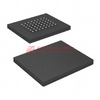
The device is packaged in a 48-TSOP I (Thin Small Outline Package) enclosure, which offers a compact and space-efficient solution for surface mount applications. The RoHS-compliant and lead-free design of the S29AL008J55TFAR20 aligns with environmental regulations, making it a sustainable choice for modern electronics.

Key features of the S29AL008J55TFAR20 include:

- 8Mb (1M x 8, 512K x 16) memory capacity

- Parallel memory interface

- 55ns access time and 55ns write cycle time

- Wide operating temperature range of -40°C to 85°C

- RoHS compliance and lead-free design

- 48-TSOP I packaging for surface mount applications

The S29AL008J55TFAR20 is well-suited for various applications, such as:

- Embedded systems

- Consumer electronics

- Industrial control and automation

- Networking and telecommunications equipment

- Automotive electronics

While there may be equivalent or alternative models available from other manufacturers, the S29AL008J55TFAR20 from Cypress Semiconductor stands out as a reliable and high-performance NOR flash memory solution, offering a combination of features, compatibility, and environmental compliance to meet the demands of modern electronic systems.

S29AL008J55TFAR20 Image
S29AL008J55TFAR20 (1)

S29AL008J55TFAR20 Key Technical Attributes

Manufacturer Part Number - S29AL008J55TFAR20

Manufacturer - Cypress Semiconductor

Technology - FLASH - NOR

S29AL008J55TFAR20 Packing Size

Packaging Type - Tray

Package / Case - 48-TFSOP (0.724", 18.40mm Width)

Encapsulation - TSOP48

Supplier Device Package - 48-TSOP I

S29AL008J55TFAR20 Application

This memory IC is suitable for a wide range of applications that require data storage, code storage, or boot memory in sectors such as consumer electronics, automotive, and computer peripherals.

S29AL008J55TFAR20 Features

The S29AL008J55TFAR20 is a FLASH - NOR Memory IC with a memory size of 8Mb configurable as 1M x 8 or 512K x 16. It offers an access time and write cycle time of 55 nanoseconds, which facilitates fast read and write operations. This memory IC operates within a voltage supply range of 3 V to 3.6 V and can function efficiently in a temperature range from -40°C to 85°C. It's designed for surface mount technology.

S29AL008J55TFAR20 Quality and Safety Features

The memory IC adheres to RoHS compliance, which means it is lead-free and meets current environmental standards regarding hazardous materials. It also has a Moisture Sensitivity Level (MSL) of 3, ensuring robust performance for up to 168 hours under exposure to moisture.

S29AL008J55TFAR20 Compatibility

The S29AL008J55TFAR20 integrates seamlessly into systems requiring a parallel memory interface, making it highly compatible with traditional and modern microcontrollers and processors in various tech environments.

S29AL008J55TFAR20 Datasheet PDF

For a comprehensive understanding of all technical parameters and application guidelines of the S29AL008J55TFAR20, customers are encouraged to download the most authoritative datasheet available on our website. This ensures you have access to accurate and detailed information directly from the manufacturer.

Quality Distributor

IC-Components is a premium distributor of Cypress Semiconductor products. We guarantee product authenticity and optimal customer service. We suggest our customers get a quote directly on our website to ensure the best deal and reliable supply continuity for the S29AL008J55TFAR20 memory IC.

Frequently Asked Questions

What are the practical considerations for interfacing the S29AL008J55TFAR20 NOR Flash with a 3.3V microcontroller that has 2.5V I/O?
Interfacing the S29AL008J55TFAR20 NOR Flash with a microcontroller operating at 2.5V I/O requires careful attention to voltage level shifting. While the S29AL008J55TFAR20 supports a VCC of 3V to 3.6V, its I/O pins are typically not 5V tolerant. Direct connection to a 2.5V microcontroller's I/O may result in unreliable communication due to insufficient drive strength or potential voltage mismatches. Implementing a bi-directional level shifter, such as a TXB0108 or similar, is highly recommended for ensuring robust and stable data transfer between the 3.3V flash memory and the 2.5V microcontroller. This prevents potential damage to the microcontroller's I/O pins and guarantees proper signal integrity for both read and write operations of the S29AL008J55TFAR20.
How does the S29AL008J55TFAR20's 55ns access time impact real-time embedded system performance, and what are typical applications where this speed is sufficient or limiting?
The 55ns access time of the S29AL008J55TFAR20 NOR Flash dictates the minimum clock speed required for direct code execution or efficient data retrieval. For systems where boot-up sequences or critical instruction fetches occur at rates that can tolerate this latency, the S29AL008J55TFAR20 is suitable. Applications like basic industrial control systems, simple display drivers, or configurations where the flash is primarily used for firmware storage and infrequent data access will find the S29AL008J55TFAR20 adequate. However, for high-performance real-time applications demanding sub-20ns access times for instruction fetching, such as advanced signal processing, high-speed data acquisition, or complex GUI rendering, the 55ns access time of the S29AL008J55TFAR20 may become a bottleneck, necessitating the consideration of faster NOR flash devices.
When migrating from an older 5V NOR flash to the S29AL008J55TFAR20, what are the primary electrical and layout challenges to anticipate?
Migrating from a 5V NOR flash to the S29AL008J55TFAR20, which operates at 3V, presents significant electrical and layout challenges. The most critical electrical change is the voltage requirement; a direct replacement without voltage regulation will damage the S29AL008J55TFAR20. A reliable 3V power supply must be implemented. Furthermore, the parallel interface signals might have different drive strengths and logic levels, requiring level shifting if the host system remains at 5V. Layout considerations for the S29AL008J55TFAR20 in its 48-TSOP I package will differ from older packages, demanding updated footprint definitions. Signal integrity is paramount; ensure proper decoupling capacitors are placed close to the S29AL008J55TFAR20's power pins and that trace impedance is matched to minimize reflections, especially at higher operating frequencies.
What are the implications of the S29AL008J55TFAR20's 8Mb memory size and 1M x 8 / 512K x 16 organization for firmware updates and data storage in embedded systems?
The 8Mb memory size of the S29AL008J55TFAR20, with its flexible 1M x 8 or 512K x 16 organization, offers sufficient space for many embedded firmware applications. The 1M x 8 configuration is standard for byte-addressable systems, while the 512K x 16 mode can offer faster read operations for 16-bit data architectures. For firmware updates, the erase block size (not specified but typical for NOR flash) will influence the efficiency of partial updates; larger erase blocks mean more data is erased and rewritten even for small changes. Designers using the S29AL008J55TFAR20 should consider its program/erase endurance ratings (typically in the tens of thousands of cycles for NOR flash) when designing update mechanisms to ensure long-term reliability. If extensive frequent data logging is required beyond firmware, the 8Mb size might be a limitation, and external non-volatile storage like EEPROM or NAND flash might be more appropriate.
Under what operating conditions, particularly in industrial environments with temperature fluctuations (-40°C to 85°C), should designers be cautious about the S29AL008J55TFAR20's long-term reliability and data retention?
The S29AL008J55TFAR20 is rated for operation from -40°C to 85°C, which covers most industrial temperature ranges. However, prolonged operation at the extremes of this range, especially high temperatures, can accelerate wear-out mechanisms and potentially impact data retention over extended periods. While NOR flash generally offers good data retention (often 10-20 years at room temperature), this can be reduced at elevated temperatures. Designers should ensure adequate thermal management in their enclosures to keep the S29AL008J55TFAR20 within a reasonable operating temperature envelope to maximize its lifespan and data integrity. Regular data integrity checks, if feasible in the application, can also be a prudent measure for critical systems operating under harsh conditions.
Can the S29AL008J55TFAR20 be used as a direct replacement for other 8Mb NOR flash parts, and what potential compatibility issues should be assessed with specific part numbers like the AM29LV800BB-90EF?
While the S29AL008J55TFAR20 is an 8Mb NOR flash with a parallel interface, direct drop-in replacement for other specific parts like the AM29LV800BB-90EF requires careful validation. Key compatibility aspects to assess include exact pinouts (though both are 48-TSOP), command set compatibility (especially for programming and erase sequences), voltage requirements (ensure the S29AL008J55TFAR20's 3V compatibility aligns with the host system's needs), and electrical characteristics such as access time and bus width support (e.g., 16-bit mode). Some older flash devices might have proprietary command sets or slightly different timing requirements that the S29AL008J55TFAR20 may not perfectly emulate. It's crucial to consult the datasheets of both the S29AL008J55TFAR20 and the original part to identify any functional or timing discrepancies before committing to a replacement.
What are the implications of the S29AL008J55TFAR20's 48-TSOP I encapsulation for board layout and manufacturing assembly processes?
The S29AL008J55TFAR20's 48-TSOP I (Thin Small Outline Package) encapsulation requires specific considerations for board layout and manufacturing. The package has a relatively wide body (0.724", 18.40mm) and leads with a specific pitch, demanding a corresponding footprint on the PCB. Proper lead-to-pad soldering is critical for good electrical contact and mechanical strength. During board layout for the S29AL008J55TFAR20, ensure sufficient clearance around the component to avoid bridging during reflow soldering and to allow for automated optical inspection (AOI). Manufacturing assembly processes must be compatible with TSOP packages; care should be taken to manage potential package warping during reflow, especially for trays of parts. Moisture sensitivity level (MSL 3) indicates that the S29AL008J55TFAR20 needs to be handled within a specified timeframe after de-bagging and stored appropriately to prevent premature failure during soldering.

Recent Reviews

Leave Comment
Hello, you have not logged in, please log in
User Login

Forgot password?

No account yet? Register now

Tips
Please speak legally
Your email will be hidden
Please complete all required fields ( denoted with* )
Mark
5.0

You May Also Be Interested In:


S29AL008J55TFAR20

S29AL008J55TFAR20

Spansion

IC FLASH 8MBIT PARALLEL 48TSOP

In Stock: 8596

SUBMIT RFQ