Choose your country or region.

SI8808DB-T2-E1.jpg ImageView larger image
Image may be representation.
See specs for product details.

MAX40200ANS+

In Stock 58165 pcs Reference Price(In US Dollars)
1+
$0.3636
Manufacturer Part Number:
MAX40200ANS+
Manufacturer / Brand
Analog Devices Inc./Maxim Integrated
Part of Description:
CURRENT SENSE/IDEAL DIODE
Datasheets:
MAX40200ANS+(1).pdfMAX40200ANS+(2).pdfMAX40200ANS+(3).pdfMAX40200ANS+(4).pdfMAX40200ANS+(5).pdfMAX40200ANS+(6).pdfMAX40200ANS+(7).pdf
Lead Free Status / RoHS Status:
ROHS3 Compliant
Stock Condition:
New original, 58165 pcs Stock Available.
ECAD Model:
Ship From:
Hong Kong
Shipment Way:
DHL/Fedex/TNT/UPS

Inquiry Online

Please complete all required fields with your contact information.Click "SUBMIT REQUEST" we will contact you shortly by email. Or Email us: Info@IC-Components.com
Part Number
Manufacturer
Require Quantity
Target Price(USD)
Company Name
Contact Name
E-mail
Phone
Message
Please enter Verify Code and click "Submit"
Part Number MAX40200ANS+
Manufacturer / Brand Analog Devices Inc./Maxim Integrated
Stock Quantity 58165 pcs Stock
Category Integrated Circuits (ICs) > Power Management (PMIC) - OR Controllers, Ideal Diodes
Description CURRENT SENSE/IDEAL DIODE
Lead Free Status / RoHS Status: ROHS3 Compliant
Voltage - Supply 1.5V ~ 5.5V
Type Source Selector Switch
Supplier Device Package 4-WLP (0.73x0.73)
Series -
Ratio - Input:Output 1:1
Package / Case 4-XFBGA, WLBGA
Package Strip
Operating Temperature -40°C ~ 125°C
Mounting Type Surface Mount
Internal Switch(s) Yes
FET Type P-Channel
Delay Time - ON 65 µs
Delay Time - OFF 1.6 ms
Current - Supply 7 µA
Current - Output (Max) 1.2A
Base Product Number MAX40200
Applications Handheld/Mobile Devices

Packaging & ESD

Industry-standard static shielding packaging is used for electronic components.Anti-static, light-transparent materials allow easy identification of ICs and PCB assemblies.
The packaging structure provides electrostatic protection based on Faraday cage principles.This helps protect sensitive components from static discharge during handling and transportation.


All products are packed in ESD-safe anti-static packaging. Outer packaging labels include part number, brand, and quantity for clear identification. Goods are inspected prior to shipment to ensure proper condition and authenticity.

ESD protection is maintained throughout packing, handling, and global transportation. Secure packaging provides reliable sealing and resistance during transit. Additional cushioning materials are applied when required to protect sensitive components.

QC(Part Testing by IC Components)Quality Warranty

We can offer worldwide express delivery service, such as DHLor FedEx or TNT or UPS or other forwarder for shipment.

Global Shipment by DHL/FedEx/TNT/UPS

Shipping Fees reference DHL/FedEx
1). You can offer your express delivery account for shipment, ifyou haven’t any express account for shipment, we can offer our account inadvance.
2). Use our account for shipment, Shipment charges(Reference DHL/FedEx, Different Countries has different price.)
Shipment charges: (Reference DHL and FedEX)
Weight(KG): 0.00kg-1.00kg Price(USD$) : USD$60.00
Weight(KG): 1.00kg-2.00kg Price(USD$) : USD$80.00
* The price of cost is reference with DHL/FedEx. The detail charges, please contact us. Different country the express charges are different.


We accept the payment terms: Telegraphic Transfer(T/T), Credit Card, PayPal and Western Union.

PayPal:

PayPal Bank Information:
Company Name : IC COMPONENTS LTD
Paypal ID: PayPal@IC-Components.com

BANK TRANSFAR (Telegraphic Transfer)

Payment For Telegraphic Transfers:
Company Name : IC COMPONENTS LTD Beneficiary Account Number : 549-100669-701
Beneficiary Bank name : Bank of Communications (Hong Kong) Ltd Beneficiary Bank Code : 382 (for local payment)
Beneficiary Bank SWIFT : COMMHKHK
Beneficiary Bank Address : Tsuen Wan Market Street Branch 53 Market Street, Tsuen Wan N.T., Hong Kong

Any inquires or questions, please kindly contact us Email: Info@IC-Components.com


MAX40200ANS+ Product Details:

The MAX40200ANS+ from Analog Devices/Maxim Integrated is a sophisticated current sense and ideal diode integrated circuit designed specifically for power management applications in handheld and mobile devices. This advanced semiconductor solution belongs to the Power Management IC (PMIC) category, specifically functioning as an OR controller and ideal diode, addressing critical design challenges in modern portable electronics where efficient power routing and protection are essential.

This innovative device operates as a source selector switch, intelligently managing power flow between multiple input sources while providing comprehensive protection against reverse current flow. The IC incorporates internal P-Channel FET switches capable of handling up to 7A supply current with a maximum output current of 1.2A, making it ideal for applications requiring robust power management in space-constrained environments. The device operates across a wide supply voltage range of 1.5V to 5.5V, accommodating various battery and power supply configurations commonly found in portable electronics.

The MAX40200ANS+ features precise timing control with a 65-second ON delay and rapid 1.6ms OFF delay, ensuring optimal power sequencing and protection. Its compact 4-WLP (Wafer Level Package) measuring just 0.73x0.73mm addresses the critical space constraints in modern mobile device designs while maintaining excellent thermal performance across an operating temperature range of -40°C to 125°C. The surface mount configuration and ultra-miniature WLBGA package make it perfectly suited for high-density PCB layouts where board real estate is at a premium.

This device excels in handheld and mobile device applications where multiple power sources such as USB chargers, wireless charging systems, and batteries need to be seamlessly managed. The integrated current sensing capability provides real-time monitoring of power consumption, enabling intelligent power management decisions and extending battery life. The ideal diode functionality eliminates the voltage drop associated with traditional Schottky diodes while providing superior reverse current protection.

The MAX40200ANS+ is RoHS3 compliant, meeting current environmental regulations for lead-free manufacturing. Its 0:55 input-to-output ratio specification indicates its specialized switching architecture optimized for power routing applications. The device's internal switch configuration eliminates the need for external components, reducing overall system cost and complexity while improving reliability.

Equivalent and alternative models in this category include the Texas Instruments TPS2121, which offers similar dual-input power switching functionality, and the ON Semiconductor NCP4200, providing comparable ideal diode and power management features. The Linear Technology LTC4415 series presents another alternative with similar current sensing and power path management capabilities. Maxim's own MAX40200 family includes variants like the MAX40200AUK+ in different package options, while competitors such as the Analog Devices ADP5090 and the Intersil ISL9220 offer related power management solutions with varying current handling capabilities and package configurations. These alternatives may differ in specific parameters such as current ratings, package sizes, or additional integrated features, making the selection dependent on specific application requirements and design constraints.
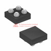
MAX40200ANS+ Image
MAX40200ANS+ (1)

MAX40200ANS+ Key Technical Attributes

Package: 4-WLP (0.73x0.73)

Supply Voltage: 1.5V to 5.5V

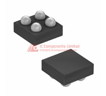
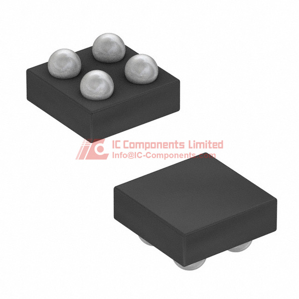
MAX40200ANS+ Packing Size

The MAX40200ANS+ is available in an ultra-compact 4-WLP (Wafer Level Package) measuring just 0.73mm x 0.73mm. This package provides a minimal footprint for space-constrained designs and optimal thermal characteristics suitable for surface-mount manufacturing. The package material is highly reliable, designed for robust operation, and supports efficient heat dissipation for demanding applications. The pin configuration enables straightforward implementation, ensuring reliability even in high-density board layouts.

MAX40200ANS+ Application

This device is tailored for use in handheld and mobile devices where efficient power management and current sense functions are crucial. It supports applications requiring ideal diode and OR controller functionalities, such as battery-powered systems, portable consumer electronics, medical devices, and wearables. The MAX40200ANS+ is particularly beneficial in solutions demanding compact size, high efficiency, and fast switching between power sources.

MAX40200ANS+ Features

The MAX40200ANS+ integrates both ideal diode and current sensing in one component, delivering precise source selection with minimal voltage drop and low quiescent current. It supports a maximum supply voltage of 5.5V and up to 1.2A continuous output current. Fast ON delay time of 65μs and fast OFF delay time of 1.6ms ensure responsive source switching during rapid load changes. Its P-Channel internal FET technology is optimized for low forward voltage, reducing power loss and enhancing battery life. ROHS3 compliance assures environmental safety and regulatory adherence. Its small footprint and surface-mount compatibility simplify PCB design for space-limited products.

MAX40200ANS+ Quality and Safety Features

The MAX40200ANS+ is ROHS3 compliant, reflecting its alignment with the latest hazardous substance restrictions for environmental protection. It operates reliably over a wide temperature range from -40°C to 125°C, ensuring safe performance in diverse operating conditions. The package provides proven reliability against mechanical stress and external environmental effects, supporting lifetime product integrity.

MAX40200ANS+ Compatibility

This component is designed for seamless integration into modern handheld/mobile architecture, and is compatible with standard surface-mount techniques and automated assembly processes. The standard 4-WLP package ensures interchangeability with other similar components and allows upgrades within the Maxim Integrated product family. The broad supply voltage range ensures suitability for various industry-standard power rails.

MAX40200ANS+ Datasheet PDF

Our website offers the most authoritative and up-to-date datasheet for the MAX40200ANS+. We strongly recommend downloading the datasheet on the current page for comprehensive technical details, design guidelines, and recommended usage practices. This ensures you have reliable reference material directly from the manufacturer.

Quality Distributor

IC-Components is a premium distributor for Analog Devices and Maxim Integrated products. Experience the advantage of sourcing authentic, high-quality MAX40200ANS+ devices with prompt delivery and full support. We invite you to get a competitive quote directly on our website—your trusted choice for the industry’s most reliable semiconductor components.

Frequently Asked Questions

How can I ensure proper power supply compatibility when integrating the MAX40200ANS+ in my handheld device?
The MAX40200ANS+ operates within a supply voltage range of 1.5V to 5.5V, so verify your design's power source stays within this range. For handheld applications, ensure a stable and noise-free voltage supply to prevent operational issues, and consider decoupling capacitors close to the device to maintain stability.
What are the key considerations for selecting the MAX40200ANS+ as an ideal diode or power switch in portable electronics?
When using the MAX40200ANS+ as an ideal diode or source selector switch, account for the maximum continuous current of 7A and the maximum output current of 1.2A. Ensure your application's load current does not exceed these ratings. Also, evaluate the voltage drops and delay times (ON delay of 65µs and OFF delay of 1.6ms) to ensure system responsiveness meets your design requirements.
How does the P-Channel FET inside the MAX40200ANS+ affect its suitability for high-current switching in power path management?
The internal P-Channel FET enables efficient high-current switching with low voltage drop, suited for managing power in handheld devices. Confirm that your load current stays within the 1.2A maximum output current and that switching delays (ON and OFF times) are acceptable within your system's timing constraints.
Can the MAX40200ANS+ operate reliably in industrial applications with temperature fluctuations from -40°C to 125°C?
Yes, the MAX40200ANS+ is rated for industrial temperature ranges from -40°C to 125°C, making it suitable for use in industrial or long-term deployed systems. Always consider additional design margin and proper thermal management to ensure reliability over the intended temperature span.
What are the implications of choosing the 4-WLP (0.73x0.73 mm) package for integrating the MAX40200ANS+ on a densely populated PCB?
The 4-WLP package provides a compact footprint ideal for space-constrained designs such as mobile devices. Be aware that its surface-mount nature and small pad size require precise PCB fabrication and assembly processes. Use appropriate reflow profiles to prevent damage and ensure proper solder joints.
How does the delay time of 65µs ON and 1.6ms OFF in the MAX40200ANS+ impact synchronization in power sequencing?
These delay times can affect power-up or power-down sequencing; the relatively quick ON delay (65µs) allows for rapid activation, while the OFF delay (1.6ms) may introduce a brief disconnect period. Design your power sequencing to accommodate these delays to prevent transient issues during state changes.
Is the MAX40200ANS+ suitable for replacing traditional diode selectors or MOSFET switches in existing designs?
Yes, the MAX40200ANS+ can replace conventional diode or MOSFET-based sources where low voltage drop, fast switching, and precise control are required. However, review the current and voltage ratings, delay times, and its FET characteristics to ensure compatibility with your specific application, especially in high-reliability environments.
What considerations should I keep in mind regarding input/output voltage levels when using the MAX40200ANS+ for signal switching?
The device supports input/output voltage ratios of 0:55, with a supply voltage range of 1.5V to 5.5V. Ensure that your system signals do not exceed these levels and that the chosen I/O voltages are compatible. Be cautious of input voltage thresholds to prevent unintended switching or malfunction.
How does the internal switch design of the MAX40200ANS+ influence its efficiency and power loss in critical applications?
The internal P-Channel FET offers low on-resistance, improving efficiency during high-current operation. Nonetheless, evaluate the conduction losses under your load conditions to optimize thermal management and prevent excessive power dissipation, especially in continuous operation scenarios.
When designing a replacement solution for the MAX40200ANS+ model, what trade-offs should I consider between different similar components?
When replacing the MAX40200ANS+ with alternative parts, compare their current ratings, switching delays, package types, temperature ranges, and internal FET characteristics. Choosing a component with similar or superior performance parameters can ensure system reliability, but consider manufacturing tolerances and compatibility with your existing PCB layout and power management architecture.

Recent Reviews

Leave Comment
Hello, you have not logged in, please log in
User Login

Forgot password?

No account yet? Register now

Tips
Please speak legally
Your email will be hidden
Please complete all required fields ( denoted with* )
Mark
5.0

You May Also Be Interested In:


MAX40200ANS+

MAX40200ANS+

Analog Devices Inc./Maxim Integrated

CURRENT SENSE/IDEAL DIODE

In Stock: 58165

SUBMIT RFQ