Choose your country or region.

10-WFDFN Exp Pkg.jpg ImageView larger image
Image may be representation.
See specs for product details.

LM5010ASD

In Stock 12230 pcs Reference Price(In US Dollars)
1000+
$3.1902
Manufacturer Part Number:
LM5010ASD
Manufacturer / Brand
Texas Instruments
Part of Description:
IC REG BUCK ADJUSTABLE 1A 10WSON
Datasheets:
LM5010ASD(1).pdfLM5010ASD(2).pdf
Lead Free Status / RoHS Status:
ROHS3 Compliant
Stock Condition:
New original, 12230 pcs Stock Available.
ECAD Model:
Ship From:
Hong Kong
Shipment Way:
DHL/Fedex/TNT/UPS

Inquiry Online

Please complete all required fields with your contact information.Click "SUBMIT REQUEST" we will contact you shortly by email. Or Email us: Info@IC-Components.com
Part Number
Manufacturer
Require Quantity
Target Price(USD)
Company Name
Contact Name
E-mail
Phone
Message
Please enter Verify Code and click "Submit"
Part Number LM5010ASD
Manufacturer / Brand Texas Instruments
Stock Quantity 12230 pcs Stock
Category Integrated Circuits (ICs) > Power Management (PMIC) - Voltage Regulators - DC DC Switching Regulators
Description IC REG BUCK ADJUSTABLE 1A 10WSON
Lead Free Status / RoHS Status: ROHS3 Compliant
Voltage - Output (Min/Fixed) 2.5V
Voltage - Output (Max) 70V
Voltage - Input (Min) 6V
Voltage - Input (Max) 75V
Topology Buck
Synchronous Rectifier No
Supplier Device Package 10-WSON (4x4)
Series -
Package / Case 10-WDFN Exposed Pad
Package Tape & Reel (TR)
Output Type Adjustable
Output Configuration Positive
Operating Temperature -40°C ~ 150°C (TJ)
Number of Outputs 1
Mounting Type Surface Mount
Function Step-Down
Frequency - Switching 100kHz ~ 1MHz
Current - Output 1A
Base Product Number LM5010

Packaging & ESD

Industry-standard static shielding packaging is used for electronic components.Anti-static, light-transparent materials allow easy identification of ICs and PCB assemblies.
The packaging structure provides electrostatic protection based on Faraday cage principles.This helps protect sensitive components from static discharge during handling and transportation.


All products are packed in ESD-safe anti-static packaging. Outer packaging labels include part number, brand, and quantity for clear identification. Goods are inspected prior to shipment to ensure proper condition and authenticity.

ESD protection is maintained throughout packing, handling, and global transportation. Secure packaging provides reliable sealing and resistance during transit. Additional cushioning materials are applied when required to protect sensitive components.

QC(Part Testing by IC Components)Quality Warranty

We can offer worldwide express delivery service, such as DHLor FedEx or TNT or UPS or other forwarder for shipment.

Global Shipment by DHL/FedEx/TNT/UPS

Shipping Fees reference DHL/FedEx
1). You can offer your express delivery account for shipment, ifyou haven’t any express account for shipment, we can offer our account inadvance.
2). Use our account for shipment, Shipment charges(Reference DHL/FedEx, Different Countries has different price.)
Shipment charges: (Reference DHL and FedEX)
Weight(KG): 0.00kg-1.00kg Price(USD$) : USD$60.00
Weight(KG): 1.00kg-2.00kg Price(USD$) : USD$80.00
* The price of cost is reference with DHL/FedEx. The detail charges, please contact us. Different country the express charges are different.


We accept the payment terms: Telegraphic Transfer(T/T), Credit Card, PayPal and Western Union.

PayPal:

PayPal Bank Information:
Company Name : IC COMPONENTS LTD
Paypal ID: PayPal@IC-Components.com

BANK TRANSFAR (Telegraphic Transfer)

Payment For Telegraphic Transfers:
Company Name : IC COMPONENTS LTD Beneficiary Account Number : 549-100669-701
Beneficiary Bank name : Bank of Communications (Hong Kong) Ltd Beneficiary Bank Code : 382 (for local payment)
Beneficiary Bank SWIFT : COMMHKHK
Beneficiary Bank Address : Tsuen Wan Market Street Branch 53 Market Street, Tsuen Wan N.T., Hong Kong

Any inquires or questions, please kindly contact us Email: Info@IC-Components.com


LM5010ASD Product Details:

The LM5010ASD is a high-performance buck voltage regulator integrated circuit designed by Luminary Micro/Texas Instruments, specifically engineered for precision power management in demanding electronic applications. This robust device offers exceptional voltage step-down capabilities, allowing efficient power conversion across a wide input voltage range of 6V to 75V, with the ability to produce a highly flexible adjustable output voltage from 2.5V up to 70V.

Engineered for versatility, the IC can handle up to 1A of output current and operates across an impressive temperature range of -40°C to 150°C, making it suitable for extreme environmental conditions. The device utilizes a buck topology for efficient voltage reduction, switching at frequencies between 100kHz and 1MHz, which enables compact and high-efficiency power supply designs.

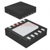
The LM5010ASD is a surface-mount component packaged in a 10-WSON (4x4) format, designed for easy integration into modern electronic systems. Its positive output configuration and single-output design make it ideal for applications requiring precise voltage regulation, such as automotive electronics, industrial control systems, telecommunications equipment, and portable electronic devices.

Key advantages include its wide input voltage tolerance, robust thermal performance, and compact form factor. The device does not incorporate a synchronous rectifier, which simplifies its design while maintaining reliable performance. Potential equivalent or alternative models might include similar buck regulators from manufacturers like Linear Technology, Analog Devices, or other Texas Instruments product lines with comparable specifications.

Professionals in power electronics, embedded systems design, and circuit engineering will find this integrated circuit particularly valuable for creating efficient, compact power management solutions across various technological platforms.

LM5010ASD Image
LM5010ASD (1)

LM5010ASD Key Technical Attributes

Integrated Circuit (IC) Regulator Buck Adjustable

Output Current 1A

Output Power 10W

Operating Temperature Range -40°C to 150°C (junction temperature)

Switching Frequency Range 100kHz to 1MHz

Input Voltage Range 6V to 75V

Output Voltage Range 2.5V (minimum) up to 70V

Topology Step-Down (Buck) Regulator

Number of Outputs 1

Output Configuration Positive, Adjustable Voltage

Synchronous Rectifier Not included

LM5010ASD Packing Size

Package Type 10-WSON (4x4 mm) surface-mount device

Encapsulation 10-WDFN with Exposed Pad for improved thermal dissipation

Material Lead-frame based IC packaging designed for high thermal conductivity

Pin Configuration 10 pins optimized for power and signal handling in compact format

Mounting Type Surface Mount Technology (SMT) suitable for automated PCB assembly

Packaging Method Tape & Reel (TR) for efficient pick-and-place processing

LM5010ASD Application

Designed for power management circuits requiring efficient step-down voltage regulation

Suitable for industrial and automotive systems operating within wide voltage input range

Ideal for embedded power supplies in communication equipment, instrumentation, and control devices

Used in point-of-load conversion applications where space and thermal management are critical

LM5010ASD Features

Adjustable output voltage allowing flexible design and use in diverse systems

Supports high input voltage up to 75V, enabling compatibility with harsh electrical environments

Operating frequency range up to 1MHz to optimize size and efficiency of external inductors and capacitors

Low quiescent current improving overall system power efficiency and battery life in portable applications

Exposed pad package enhances heat dissipation, supporting high power density designs

Built-in protection features such as thermal shutdown and undervoltage lockout to ensure device reliability

Stable operation over the full temperature range of -40°C to 150°C, suitable for demanding environments

Compact 4x4 mm footprint suitable for space-constrained electronic designs

Designed without synchronous rectification, simplifying external component requirements and cost

LM5010ASD Quality and Safety Features

Manufactured by Luminary Micro / Texas Instruments, a globally recognized semiconductor supplier known for rigorous quality control

Complies with RoHS requirements, ensuring environmental safety and restriction of hazardous substances

Exposed pad package design for high thermal efficiency, reducing risks of overheating and prolonging device life

Robust operating temperature range supports safe use in industrial and automotive applications under extreme conditions

Quality verification procedures ensure consistent electrical and thermal performance

Internal protection mechanisms prevent damage from thermal stress and abnormal operating conditions

LM5010ASD Compatibility

Compatible with standard surface-mount PCB assembly processes and footprints for 10-WSON packages

Works effectively with common PWM controller architectures and external passive components such as inductors, diodes, and capacitors

Can be integrated seamlessly into existing power management systems requiring adjustable step-down regulation

Suitable for operation with a broad range of input power sources from 6V up to 75V, including battery and unregulated DC inputs

LM5010ASD Datasheet PDF

Our website provides the most authoritative and up-to-date datasheet for the LM5010ASD model, containing detailed specifications, electrical characteristics, application guidelines, and layout recommendations.

Customers are strongly encouraged to download the datasheet directly from this page to ensure access to accurate technical information for optimal design and implementation.

Quality Distributor

IC-Components stands as a premium distributor of Texas Instruments products, including the LM5010ASD, offering reliable sourcing and expert customer service.

We invite customers to request a competitive quote on our website, benefiting from our extensive inventory and fast delivery options.

Partner with IC-Components for guaranteed genuine parts, professional support, and the best pricing on this and other high-quality integrated circuits.

Frequently Asked Questions

When designing a DC-DC converter with an input voltage up to 75V and requiring an adjustable output between 2.5V and 70V at 1A, how does the LM5010ASD's 100kHz-1MHz switching frequency range impact component selection for external passive components like inductors and capacitors in a buck topology?
The LM5010ASD's flexible switching frequency of 100kHz to 1MHz allows for significant trade-offs in external component selection for its buck topology. A higher switching frequency, closer to 1MHz, enables the use of smaller inductor and capacitor values, which can reduce overall board space and cost, particularly beneficial for compact designs. However, operating at higher frequencies can lead to increased switching losses in the LM5010ASD and other components, potentially impacting efficiency and thermal management. Conversely, operating at lower frequencies, around 100kHz, generally results in higher efficiency due to reduced switching losses, but requires larger inductor and capacitor values, increasing the physical footprint and potential cost of these components. When selecting these passives for the LM5010ASD, consider the required output ripple, transient response, and the power dissipation of the chosen inductor (core losses and DC resistance) and capacitors (Equivalent Series Resistance - ESR). It's crucial to ensure the chosen inductor has a saturation current rating well above the peak inductor current to prevent saturation, and the capacitors have sufficient ripple current handling capability.
For industrial automation applications requiring a stable 1A adjustable output from a 6V to 75V input range, what are the key reliability considerations when using the LM5010ASD, especially concerning its -40°C to 150°C junction temperature (TJ) rating and the 10-WSON package?
The LM5010ASD's wide operating temperature range of -40°C to 150°C junction temperature (TJ) makes it suitable for many industrial environments. However, achieving reliable operation at the higher end of this range requires careful thermal design. The 10-WSON (4x4) package has an exposed pad for heat sinking, which is critical for dissipating heat generated by the LM5010ASD. To ensure reliability in demanding industrial applications, a robust thermal management strategy must be implemented. This includes proper PCB layout with sufficient copper area connected to the exposed pad for thermal spreading, and potentially the use of thermal vias to conduct heat to internal or bottom layers. Calculating the expected junction temperature under worst-case operating conditions (maximum input voltage, maximum load current, and ambient temperature) is essential. The LM5010ASD's efficiency, along with the power dissipation of external components, will contribute to the overall thermal load. Ensuring the junction temperature remains well below the 150°C TJ limit is paramount for long-term operational stability and to prevent premature component failure.
I'm looking to replace an older buck converter IC in a system that expects a positive adjustable output voltage. Can the LM5010ASD be considered as a direct or near-direct drop-in replacement for parts like the LT3757, assuming similar current and voltage specifications? What are the primary design implications of such a migration?
While the LM5010ASD shares the buck topology and an adjustable positive output capability with devices like the LT3757, it's unlikely to be a direct drop-in replacement without redesign. Key differences to consider for a migration to the LM5010ASD include: * **Pinout and Package:** The LM5010ASD is in a 10-WSON (4x4) package, while other ICs might have different pinouts and package sizes. Re-routing PCB traces will almost certainly be necessary. * **Switching Frequency and External Components:** The LM5010ASD's switching frequency range (100kHz-1MHz) may differ from the LT3757. This difference will necessitate recalculating and potentially resizing external inductor and capacitor values. Inductor saturation current and ESR are critical re-evaluation points. * **Control Loop and Compensation:** The internal compensation networks and loop stability characteristics of the LM5010ASD may differ from the LT3757. This could require adjustments to the compensation components (resistors and capacitors) to ensure stable operation and desired transient response. * **Soft-Start and Enable:** The LM5010ASD's soft-start mechanism and enable pin functionality might not directly map to the LT3757. Ensure these features are correctly implemented in the new design. * **Efficiency and Power Dissipation:** While both are buck converters, their peak efficiencies and power dissipation profiles can vary. Re-evaluate the thermal design based on the LM5010ASD's performance. * **Input Voltage Range:** Confirm that the LM5010ASD's 6V-75V input range fully covers the operational requirements of the original design.
In a power supply design for a battery-powered sensor node where input voltage can fluctuate significantly, down to 6V, and a stable 3.3V output at up to 1A is needed, what specific concerns arise when using the LM5010ASD, particularly regarding its minimum input voltage and synchronous rectification absence?
Using the LM5010ASD for a battery-powered sensor node with a fluctuating input down to 6V requires careful consideration due to its minimum input voltage specification of 6V and the absence of synchronous rectification. The LM5010ASD is a non-synchronous buck converter. This means it uses a diode for rectification, which introduces a forward voltage drop (typically around 0.7V to 1V, depending on the diode chosen and current). This diode drop is in series with the output voltage, meaning the effective minimum output voltage achievable is higher than the theoretically calculated minimum for a synchronous converter. For a target 3.3V output, the minimum input voltage required will be approximately (Vout + Vf_diode + voltage drop across inductor) at maximum load. If the battery voltage drops close to 6V, the LM5010ASD might struggle to maintain regulation or might operate inefficiently due to the diode drop. Furthermore, the non-synchronous topology inherently has lower efficiency compared to synchronous designs, especially at lower output voltages and higher load currents, which can significantly impact battery life. It's crucial to verify that the battery's lowest expected voltage can consistently supply the LM5010ASD with enough headroom above its minimum input voltage requirement to maintain the desired 3.3V output under the maximum load.
For a system requiring an output voltage that can be dynamically adjusted between 5V and 48V, and an input supply that can vary from 12V to 60V, how can the LM5010ASD be configured to achieve this broad output range, and what are the potential efficiency limitations of such a wide-range adjustable output in a single-stage buck topology?
The LM5010ASD is designed for adjustable output voltages, but achieving such a broad range from 5V to 48V from a 12V to 60V input presents significant challenges and efficiency limitations for a single-stage buck topology. The LM5010ASD's output voltage is set by an external resistor divider from the feedback (FB) pin to ground. To cover this wide output range, the ratio of these resistors would need to change dynamically, typically controlled by a digital potentiometer or DAC, which adds complexity. The primary efficiency limitation arises from the duty cycle. For a buck converter, Duty Cycle (D) ≈ Vout / Vin. * When Vin is high and Vout is low (e.g., Vin=60V, Vout=5V), D is very small. The controller needs to pulse the switch for very short durations. * When Vin is low and Vout is high (e.g., Vin=12V, Vout=48V), D is large (D = 48/12 = 4). This is where the LM5010ASD's topology is limited. A standard buck converter cannot produce an output voltage higher than its input voltage; this configuration suggests a boost or buck-boost function is needed. Given the requirement of Vout > Vin (e.g., 48V from 12V), the LM5010ASD, being a pure buck converter, **cannot** achieve this. For the scenario where Vout < Vin (e.g., 5V from 60V or 5V from 12V), the efficiency will be lower at extreme duty cycles. Very low duty cycles can lead to increased switching losses relative to conduction losses, and very high duty cycles (approaching 1) in a non-synchronous buck can result in lower efficiency due to the diode drop becoming a significant portion of the output voltage. If the requirement truly includes Vout > Vin, the LM5010ASD is not suitable. If it's strictly Vout < Vin and Vout is adjustable over a wide range, efficiency will vary considerably, with optimal efficiency typically occurring closer to 50% duty cycle.
When integrating the LM5010ASD into a noise-sensitive analog signal processing system, what are the best practices for minimizing switching noise injected into the output, considering its 100kHz-1MHz switching frequency and non-synchronous nature?
Minimizing switching noise from the LM5010ASD in noise-sensitive analog systems is crucial and requires careful design. The non-synchronous nature means a switching diode is involved, which can generate significant high-frequency noise. Key practices include: * **Layout Optimization:** Place the LM5010ASD and its associated input/output filter components as close together as possible to minimize parasitic inductance in high-current loops (e.g., Vin -> Switch -> Inductor -> Output Capacitor -> Ground and Vin -> Switch -> Diode -> Output Capacitor -> Ground). Use short, wide traces for these critical paths. * **Output Filtering:** Implement a robust output filter. This typically involves a low-ESR output capacitor (e.g., ceramic or tantalum with sufficient ripple current rating) placed directly across the output terminals. An additional LC filter stage (a second inductor and capacitor) can further attenuate switching ripple if needed for very sensitive applications. * **Input Filtering:** Proper input filtering is also essential to prevent switching noise from propagating back to the input power source. A combination of a ceramic capacitor close to the IC's input pins and a larger bulk capacitor (electrolytic or polymer) is recommended. * **Snubber Circuits:** While not always necessary, a small RCD snubber circuit across the freewheeling diode can help damp ringing and reduce EMI, especially if the diode exhibits significant reverse recovery characteristics. * **Ferrite Beads:** Strategic placement of ferrite beads in series with the output can provide additional high-frequency impedance, further filtering noise. * **Shielding:** For extremely sensitive applications, consider localized shielding around the switching power supply section. * **Component Selection:** Choose low-ESR capacitors and inductors with good ferrite materials to minimize losses and parasitic effects.
If a higher current output (e.g., 2A) is required than the LM5010ASD's 1A rating, are there any alternative Texas Instruments or Luminary Micro parts within the LM5010 family or similar series that offer a higher current capability but maintain similar voltage and switching frequency characteristics, and what are the potential design implications of switching to a different part?
Yes, for applications requiring higher current output than the LM5010ASD's 1A rating, Texas Instruments offers other parts within the LM50xx family or similar families that provide higher current capabilities. For instance, you might look at parts like the LM5010-Q1 (automotive grade, same current) or potentially explore devices like the LM5118 (3A), LM5117 (3A), or higher current variants if available in similar package types or pin-compatible families, always verifying the datasheet. When switching to a higher current part, the primary design implications include: * **Increased Current Handling:** The new IC and its external components (especially the inductor, output capacitor, and freewheeling diode) must be rated for the higher output current and peak inductor current. * **Thermal Management:** Higher current operation typically means increased power dissipation. The new part and the overall design will require more robust thermal management, potentially necessitating a larger heatsink area on the PCB or more advanced cooling solutions. * **Component Sizing:** Inductor saturation current, DC resistance (DCR), and current rating of the output capacitors will need to be re-evaluated and likely increased. * **Switching Frequency and Control Loop:** While some higher-current parts might offer similar switching frequency ranges, their internal control loop compensation and transient response characteristics might differ. This could require adjustments to the external compensation network to maintain stability and desired performance. * **Input Voltage Range and Efficiency:** Verify that the alternative part's input voltage range is compatible with your application and compare its efficiency curves to understand any potential impact on power consumption and battery life. * **Pinout and Package:** Even within the same family, pinouts and package types can vary. A migration might require significant PCB layout changes. Always compare the datasheet carefully for pin function and package dimensions.

Recent Reviews

Leave Comment
Hello, you have not logged in, please log in
User Login

Forgot password?

No account yet? Register now

Tips
Please speak legally
Your email will be hidden
Please complete all required fields ( denoted with* )
Mark
5.0

You May Also Be Interested In:


LM5010ASD

LM5010ASD

Texas Instruments

IC REG BUCK ADJUSTABLE 1A 10WSON

In Stock: 12230

SUBMIT RFQ