The XC9802B323ER-G from Torex Semiconductor Ltd is a compact boost switching regulator designed to deliver a fixed 3.2V output at up to 80mA from input voltages ranging from 1.8V to 5.5V. Operating with a 300kHz switching frequency, this device addresses voltage step-up requirements in battery-powered and low-voltage systems where efficient DC-DC conversion is needed within a minimal footprint. The regulator accepts a broad input range that accommodates single-cell lithium batteries, AA/AAA alkaline configurations, and logic-level supply rails, making it suitable for portable instruments, sensor modules, and embedded systems where headroom is limited.
Packaged in an 8-XDFN exposed pad format measuring approximately 2.0mm × 2.0mm with a 0.5mm pitch, the XC9802B323ER-G occupies roughly half the board area of conventional SOT-23-5 step-up regulators while offering improved thermal dissipation through its ground-connected exposed pad. This thermal path becomes relevant in continuous operation near the 80mA output limit or when operating across the full -40°C to 85°C temperature range. The exposed pad also reduces ground inductance, which contributes to stable switching performance and lower EMI in noise-sensitive layouts. Surface mount assembly is straightforward, with MSL-1 rating allowing unlimited floor life after bag opening, reducing storage constraints in high-mix production environments.
The 3.2V fixed output voltage directly supports low-dropout linear regulators that require a stable upstream rail, white LED backlighting in single-string configurations, and legacy 3.3V peripherals interfaced from modern 1.8V or 2.5V system voltages. The 80mA output current capacity covers microcontroller clusters, low-power wireless transceivers, and MEMS sensors without requiring additional bulk capacitance or multi-stage conversion. The topology does not incorporate synchronous rectification, instead relying on an external Schottky diode for the freewheeling path, which simplifies external component selection and reduces solution cost in space-constrained applications where efficiency in the 75–85% range is acceptable.
At 300kHz switching frequency, the XC9802B323ER-G balances inductor size against switching losses. This frequency permits the use of 4.7µH to 10µH inductors in 1210 or 1612 case sizes, maintaining a low-profile power stage suitable for wearable devices, IoT edge nodes, and handheld instrumentation. Input and output capacitors in the 4.7µF to 10µF range, typically ceramic X5R or X7R dielectrics, provide adequate ripple filtering while meeting the stability criteria outlined in the datasheet. The part's positive output configuration and single-output architecture streamline power tree design in systems where multiple voltage domains are sourced from separate regulators rather than a single multi-output converter.
The XC9802 series is positioned for applications where board space, component count, and cost converge as primary constraints. The fixed 3.2V output eliminates the feedback resistor divider network present in adjustable boost regulators, reducing BOM by two components and freeing additional routing channels on dense PCBs. This fixed-voltage approach also removes the possibility of output drift due to resistor tolerance or temperature coefficient, ensuring consistent downstream supply voltage across production lots and environmental conditions. Compliance with RoHS3 and REACH regulations, combined with ECCN EAR99 classification, supports global distribution and integration into commercial and industrial products without export licensing complexity.
Replacing the Torex Semiconductor XC9802B323ER-G 3.2V Boost Regulator Without Creating Power-Rail Risk
Finding an equivalent or alternative part for the Torex Semiconductor Ltd XC9802B323ER-G is usually driven by availability, lifecycle planning, cost review, PCB redesign, or the need to qualify a second source for a low-power 3.2V boost rail. The challenge is that boost regulators are rarely interchangeable by part number alone. Output voltage accuracy, startup behavior, switching frequency, package footprint, compensation approach, inductor requirements, quiescent current, and load-transient behavior all affect whether a replacement can be used safely.
The XC9802B323ER-G is a fixed 3.2V, 80mA, non-synchronous boost switching regulator in a USP-8B05 / 8-XDFN exposed-pad package. Suitable replacement evaluation should begin by separating true same-family substitutions from functional alternatives that require schematic, BOM, and PCB changes.
Common equivalent and alternative part numbers to evaluate include:
- Torex Semiconductor Ltd
XC9802B333ER-G XC9802B333ER-G
Torex Semiconductor Ltd
STEP-UP CHARGE PUMP WITH REGULAT
200000
- Microchip Technology
MCP1640T-I/CHY MCP1640T-I/CHY
Microchip Technology
IC REG BOOST ADJ 350MA SOT23-6
16100
- Texas Instruments
TPS61070DDCR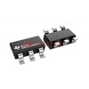 TPS61070DDCR
Texas Instruments
IC REG BOOST ADJ 500MA TSOT23-6
50400
- Analog Devices
LT1615ES5#TRMPBF LT1615ES5#TRMPBF
Analog Devices Inc.
IC REG BST SEPIC ADJ 0.3A TSOT23
21885
- onsemi
NCP1402SN33T1G NCP1402SN33T1G
onsemi
IC REG BOOST 3.3V 130MA 5TSOP
15322
These parts are not automatically drop-in replacements. Each option must be checked against the required 3.2V rail tolerance, available input voltage range, output current margin, PCB footprint, external component values, and system-level efficiency targets.
What the Torex Semiconductor XC9802B323ER-G Defines for a Compatible 3.2V Boost Replacement
The Torex Semiconductor XC9802B323ER-G belongs to the XC9802 series and is designed as a compact positive step-up DC-DC regulator. Its main electrical profile is a fixed 3.2V output, 1.8V to 5.5V input range, 80mA output current rating, 300kHz switching frequency, and non-synchronous boost topology. It operates from -40°C to 85°C and is supplied in tape-and-reel packaging for surface-mount production.
From a replacement perspective, the fixed 3.2V output is the first constraint. A 3.3V substitute may work in many logic, sensor, RF bias, or low-power analog rails, but it should not be assumed acceptable where ADC reference range, IC absolute maximum ratings, or battery-operated power budgets are tight. Adjustable alternatives can be configured to 3.2V, but they introduce feedback resistors and require layout review.
The 80mA output rating also needs practical interpretation. In a boost converter, available output current depends on input voltage, inductor saturation current, diode losses if non-synchronous, switching current limit, and thermal conditions. A replacement with a higher switch-current rating may provide better margin, but it can also require a different inductor, diode, and compensation behavior.
Mechanically, the USP-8B05 / 8-XDFN exposed-pad package is compact and thermally efficient, but it limits direct replacement choices. Many alternative boost regulators are offered in SOT-23-5, SOT-23-6, WSON, or DFN packages, so they are functional replacements rather than pin-compatible substitutes. The exposed pad, ground routing, switching-node placement, and input/output capacitor positions should be reviewed during any substitution.
Typical applications for the XC9802B323ER-G include small battery-powered equipment, sensor modules, portable instruments, low-power MCU rails, memory backup circuits, and compact embedded systems requiring a regulated 3.2V rail from a lower or variable input source. These use cases place emphasis on startup reliability, light-load efficiency, low external component count, and stable operation across temperature.
Candidate Equivalent and Alternative Parts for XC9802B323ER-G Replacement Evaluation
The following table compares practical replacement candidates for the XC9802B323ER-G. The goal is not to identify a universal substitute, but to clarify which alternatives are suitable under specific electrical, mechanical, and supply-chain conditions.
| Manufacturer | Part Number | Key Specifications | Product Features | Typical Applications | Why It Can Replace the Original Part | Main Differences or Limitations | Recommended Usage |
|---|---|---|---|---|---|---|---|
| Torex Semiconductor Ltd |
XC9802B333ER-G
Torex Semiconductor Ltd
STEP-UP CHARGE PUMP WITH REGULAT
200000
| Boost regulator, fixed 3.3V output, same XC9802 family, surface-mount package option, low-power step-up operation | Same product family behavior, similar control concept, compact package, fixed output | Low-power 3.3V logic rails, sensor power, portable devices | Closest same-family alternative when a 3.3V rail is acceptable instead of 3.2V | Output is 3.3V, not 3.2V; ordering code and package/pinout must be verified against the exact datasheet | Best first option when minimal circuit change is desired and the powered load tolerates 3.3V |
| Microchip Technology |
MCP1640T-I/CHY
Microchip Technology
IC REG BOOST ADJ 350MA SOT23-6
16100
| Synchronous boost converter, adjustable output, low-voltage startup, SOT-23-6 package, output configurable by feedback network | High efficiency at low input voltage, true shutdown options depending on variant, widely used battery boost architecture | Single-cell alkaline/NiMH/Li-ion accessory rails, portable sensors, MCU supply rails | Can be configured to 3.2V using external feedback resistors and offers more current capability than the XC9802B323ER-G in many designs | Not pin-compatible; switching frequency, compensation, inductor selection, and layout must be redesigned | Suitable when redesign flexibility exists and efficiency from low battery voltage is a priority |
| Texas Instruments |
TPS61070DDCR
Texas Instruments
IC REG BOOST ADJ 500MA TSOT23-6
50400
| Adjustable synchronous boost converter, SOT-23-6 package, wide input range, higher output-current capability than low-current boost ICs | Integrated power switch, compact external BOM, good current margin for upgraded rails | Portable instruments, wireless modules, distributed low-voltage rails | Provides a configurable 3.2V output and stronger load-current headroom than the original 80mA class device | Higher capability may require different inductor current rating and thermal review; not a footprint replacement | Suitable where the replacement must support load growth or peak-current margin |
| Analog Devices |
LT1615ES5#TRMPBF
Analog Devices Inc.
IC REG BST SEPIC ADJ 0.3A TSOT23
21885
| Micropower boost converter, adjustable output, SOT-23-5 package, high switching frequency, non-synchronous topology with external diode | Small solution size, flexible output setting, useful for compact low-current boost rails | Handheld electronics, bias supplies, small analog or sensor rails | Can generate 3.2V with feedback resistors and supports compact power conversion similar in function to the original | Requires external Schottky diode; package and circuit are different; high switching frequency changes EMI and layout requirements | Useful when a compact adjustable non-synchronous boost alternative is preferred |
| onsemi |
NCP1402SN33T1G
onsemi
IC REG BOOST 3.3V 130MA 5TSOP
15322
| Fixed 3.3V boost converter, SOT-23-5 package, PFM operation, low-voltage battery startup | Low external component count, fixed-output simplicity, light-load efficiency | Battery-powered modules, low-duty-cycle sensor circuits, small 3.3V rails | Can replace the original function when 3.3V is acceptable and the application operates from low battery input | Fixed 3.3V rather than 3.2V; input-voltage range and output-current capability differ from XC9802B323ER-G; PFM ripple behavior may differ | Suitable for low-power battery designs where ripple and load-current limits are acceptable |
Engineering Trade-Offs When Comparing XC9802B323ER-G Replacement Options
Selecting a replacement for the XC9802B323ER-G should start with the load tolerance. If the load requires exactly 3.2V, adjustable alternatives such as
MCP1640T-I/CHY
,
MCP1640T-I/CHY
Microchip Technology
IC REG BOOST ADJ 350MA SOT23-6
16100
TPS61070DDCR
, or
TPS61070DDCR
Texas Instruments
IC REG BOOST ADJ 500MA TSOT23-6
50400
LT1615ES5#TRMPBF
are more appropriate than fixed 3.3V substitutes. If the load accepts 3.3V,
LT1615ES5#TRMPBF
Analog Devices Inc.
IC REG BST SEPIC ADJ 0.3A TSOT23
21885
XC9802B333ER-G
or
XC9802B333ER-G
Torex Semiconductor Ltd
STEP-UP CHARGE PUMP WITH REGULAT
200000
NCP1402SN33T1G
may reduce design complexity, although package and behavior still need verification.
NCP1402SN33T1G
onsemi
IC REG BOOST 3.3V 130MA 5TSOP
15322
| Replacement Option | Electrical Compatibility | Mechanical Compatibility | Performance Differences | Reliability and Qualification Considerations | Package / Availability Factors | Cost and BOM Considerations | Best-Fit Scenario | Main Advantage | Main Limitation |
|---|---|---|---|---|---|---|---|---|---|
| XC9802B333ER-G | Similar same-family boost function; fixed 3.3V instead of 3.2V | Potentially closest if the same USP-8B05 package and pinout are confirmed | Similar design behavior expected, but output voltage shifts upward | Easier qualification if same family, but powered IC voltage limits must be checked | Same-family sourcing may simplify documentation | May preserve much of the original BOM if external requirements match | Existing XC9802B323ER-G designs where 3.3V is acceptable | Lowest redesign effort among listed options | Not suitable for strict 3.2V rails |
| MCP1640T-I/CHY | Adjustable to 3.2V; good low-input battery operation | Requires PCB redesign from USP-8B05 to SOT-23-6 | Synchronous topology can improve efficiency versus non-synchronous designs | Needs validation for startup, transient response, and feedback accuracy | Broadly used package, but not footprint-compatible | Adds feedback resistors; may reduce diode losses because it is synchronous | Battery-powered products needing efficient 3.2V generation | Strong efficiency and flexibility | Requires schematic and layout change |
| TPS61070DDCR | Adjustable to 3.2V with higher load-current margin | Requires new SOT-23-6 layout | Higher current capability may improve peak-load behavior | Inductor saturation current and thermal margin should be reviewed | Common package family, but no pin compatibility | May require higher-rated inductor and revised compensation/BOM | Designs where the original 80mA margin is no longer enough | Good headroom for future load increases | More design review than a same-family substitute |
| LT1615ES5#TRMPBF | Adjustable to 3.2V; non-synchronous boost architecture resembles the original concept | Requires SOT-23-5 PCB change and external diode placement | Higher switching frequency can reduce magnetics size but affects EMI | Diode selection affects efficiency, temperature rise, and output regulation | Compact package, but layout differs significantly | External Schottky diode adds BOM item and loss path | Compact low-current rails where adjustable output is needed | Flexible and space-efficient | EMI and diode-loss review required |
| NCP1402SN33T1G | Fixed 3.3V output; suitable only if 3.3V rail is allowed | Requires SOT-23-5 redesign | PFM operation may produce different ripple and load-transient behavior | Ripple-sensitive analog or RF rails require measurement | Small package and simple implementation | Low component count, but external component values may differ | Low-duty-cycle battery devices with modest load current | Simple fixed-output alternative | Not a direct 3.2V or pin-compatible replacement |
For the closest replacement path,
XC9802B333ER-G
should be checked first if the system can accept 3.3V. For an exact 3.2V rail with redesign flexibility,
XC9802B333ER-G
Torex Semiconductor Ltd
STEP-UP CHARGE PUMP WITH REGULAT
200000
MCP1640T-I/CHY
and
MCP1640T-I/CHY
Microchip Technology
IC REG BOOST ADJ 350MA SOT23-6
16100
TPS61070DDCR
are stronger functional alternatives because their outputs can be resistor-programmed.
TPS61070DDCR
Texas Instruments
IC REG BOOST ADJ 500MA TSOT23-6
50400
LT1615ES5#TRMPBF
is appropriate when an adjustable non-synchronous solution is acceptable and the external diode can be accommodated.
LT1615ES5#TRMPBF
Analog Devices Inc.
IC REG BST SEPIC ADJ 0.3A TSOT23
21885
NCP1402SN33T1G
is better suited to simple low-power 3.3V battery rails than to strict XC9802B323ER-G drop-in replacement work.
NCP1402SN33T1G
onsemi
IC REG BOOST 3.3V 130MA 5TSOP
15322
Before releasing a substitute into production, verify output voltage tolerance, startup at minimum input voltage, inductor saturation current, diode or synchronous switch losses, output ripple, thermal rise, enable/shutdown behavior, package footprint, and regulatory documentation such as RoHS status.
For pricing, availability, and sourcing support for XC9802B323ER-G replacement parts, obtain quotations through IC-Components.com or email Info@IC-Components.com.