


The EP2AGX125DF25C4N is a sophisticated field-programmable gate array (FPGA) from Intel's Arria II GX series, designed to address complex digital logic implementation challenges in modern electronic systems. This integrated circuit belongs to the embedded FPGA category and serves as a highly flexible, reconfigurable computing platform capable of handling demanding signal processing, data manipulation, and control applications.
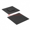
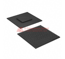
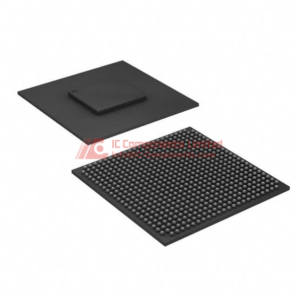
At its core, this FPGA delivers impressive computational capabilities with 118,143 logic elements and 4,964 LABs/CLBs, providing designers with substantial resources for implementing complex digital circuits and algorithms. The device features 8,315,904 total RAM bits, enabling efficient data buffering and storage for memory-intensive applications, while offering 260 I/O pins for extensive connectivity with external components and systems. The chip is housed in a compact 572-FBGA FC (Flip Chip) package measuring 25x25mm, utilizing surface mount technology for reliable board-level integration and optimized thermal performance.
This FPGA addresses several critical design challenges including the need for high-density logic integration, flexible hardware reconfiguration, and parallel processing capabilities that traditional microprocessors cannot efficiently provide. The device operates within a precise voltage supply range of 0.87V to 0.93V, contributing to reduced power consumption while maintaining high performance. Its commercial temperature range of 0°C to 85°C (junction temperature) makes it suitable for industrial and commercial applications where environmental conditions are controlled.
The primary advantages of this component include its exceptional logic density, substantial embedded memory resources, high I/O count for complex interfacing requirements, and the inherent flexibility of FPGA technology that allows for field updates and design modifications without hardware changes. The RoHS compliant status ensures environmental responsibility and regulatory compliance for modern electronics manufacturing.
This FPGA finds applications across diverse sectors including telecommunications infrastructure, industrial automation and control systems, medical imaging equipment, aerospace and defense systems, high-performance computing accelerators, video and image processing platforms, and advanced test and measurement instrumentation. The device is particularly well-suited for applications requiring custom hardware acceleration, real-time signal processing, or complex protocol implementation.
Regarding equivalent or alternative models, designers might consider other devices within Intel's Arria II GX family with different logic densities such as the EP2AGX95, EP2AGX190, or EP2AGX260 variants depending on resource requirements. Competitive alternatives from other manufacturers include Xilinx Kintex-7 series FPGAs (such as XC7K160T or XC7K325T) and Lattice ECP5 series devices, though exact pin-for-pin replacements may require design modifications. The product is available in tray packaging with a quantity of 1273 units, making it suitable for volume production requirements.
EP2AGX125DF25C4N Key Technical Attributes
FPGA with 118143 logic elements, 4964 LABs/CLBs, and total RAM bits of 8,315,904.
EP2AGX125DF25C4N Packing Size
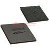
572-FBGA, FC (25x25), Tray package.
Number of I/O
260
EP2AGX125DF25C4N Application
The EP2AGX125DF25C4N FPGA from Intel’s Arria II GX series is designed for high-speed data processing, signal analysis, and embedded system applications. It is ideally suited for network infrastructure, telecommunications, medical imaging devices, industrial automation, and video processing systems, where flexible, programmable logic and high I/O capacity are critical.
EP2AGX125DF25C4N Features
This model boasts advanced 40-nm process technology, supporting a supply voltage range of 0.87V to 0.93V to optimize power efficiency. With 118,143 logic elements, 4,964 logic array blocks (LABs), and rich embedded memory totaling over 8 megabits, the EP2AGX125DF25C4N provides substantial capacity for complex computation and data buffering tasks. The 260 I/O pins allow for extensive device interconnection and system expansion. Integrated transceivers enable high-speed serial communications, making it capable of supporting PCI Express, Gigabit Ethernet, and other high-bandwidth protocols. It supports surface mount assembly, easing automated manufacturing and enhancing reliability. The FPGA’s flexibility allows for reprogramming and rapid adaptation to evolving technological requirements.
EP2AGX125DF25C4N Quality and Safety Features
RoHS compliance guarantees environmentally responsible manufacturing and meets strict regulatory standards for hazardous substances. The device operates reliably in a thermal junction temperature range of 0°C to 85°C, ensuring stable performance in commercial and industrial environments. The ball grid array (BGA) packaging with flip-chip construction enhances thermal dissipation and electrical signal integrity while minimizing noise.
EP2AGX125DF25C4N Compatibility
The EP2AGX125DF25C4N is broadly compatible with industry-standard development tools and silicon IP cores, enabling seamless integration into existing FPGA-based design environments. It supports multiple interface standards and protocols, ensuring compatibility with other digital devices and systems.
EP2AGX125DF25C4N Datasheet PDF
We encourage our customers to download the most authoritative datasheet for the EP2AGX125DF25C4N directly from this product page. Our website consistently provides the latest and most accurate technical documentation to support your design and development needs.
Quality Distributor
IC-Components is a premium distributor of Intel products. For the EP2AGX125DF25C4N FPGA, we offer genuine inventory, competitive pricing, and professional service. Request a quote today on our website for rapid and reliable procurement—where quality and customer satisfaction are always our priority.