Choose your country or region.

Cypress Semiconductor Corp
63-VFBGA.jpg ImageView larger image
Image may be representation.
See specs for product details.

S34ML01G100BHV003

Manufacturer Part Number:
S34ML01G100BHV003
Manufacturer / Brand
Cypress Semiconductor Corp
Part of Description:
IC FLASH 1GBIT PARALLEL 63BGA
Datasheets:
S34ML01G100BHV003(1).pdfS34ML01G100BHV003(2).pdfS34ML01G100BHV003(3).pdfS34ML01G100BHV003(4).pdfS34ML01G100BHV003(5).pdfS34ML01G100BHV003(6).pdfS34ML01G100BHV003(7).pdf
Lead Free Status / RoHS Status:
ROHS3 Compliant
Stock Condition:
New original, 16825 pcs Stock Available.
ECAD Model:
Ship From:
Hong Kong
Shipment Way:
DHL/Fedex/TNT/UPS

Inquiry Online

Please complete all required fields with your contact information.Click "SUBMIT REQUEST" we will contact you shortly by email. Or Email us: Info@IC-Components.com
Part Number
Manufacturer
Require Quantity
Target Price(USD)
Company Name
Contact Name
E-mail
Phone
Message
Please enter Verify Code and click "Submit"
Part Number S34ML01G100BHV003
Manufacturer / Brand Cypress Semiconductor Corp
Stock Quantity 16825 pcs Stock
Category Integrated Circuits (ICs) > Memory - Memory
Description IC FLASH 1GBIT PARALLEL 63BGA
Lead Free Status / RoHS Status: ROHS3 Compliant
Write Cycle Time - Word, Page 25ns
Voltage - Supply 2.7V ~ 3.6V
Technology FLASH - NAND
Supplier Device Package 63-BGA (11x9)
Series ML-1
Package / Case 63-VFBGA
Package Tape & Reel (TR)
Operating Temperature -40°C ~ 105°C (TA)
Mounting Type Surface Mount
Memory Type Non-Volatile
Memory Size 1Gbit
Memory Organization 128M x 8
Memory Interface Parallel
Memory Format FLASH
Base Product Number S34ML01

Packaging & ESD

Industry-standard static shielding packaging is used for electronic components.Anti-static, light-transparent materials allow easy identification of ICs and PCB assemblies.
The packaging structure provides electrostatic protection based on Faraday cage principles.This helps protect sensitive components from static discharge during handling and transportation.


All products are packed in ESD-safe anti-static packaging. Outer packaging labels include part number, brand, and quantity for clear identification. Goods are inspected prior to shipment to ensure proper condition and authenticity.

ESD protection is maintained throughout packing, handling, and global transportation. Secure packaging provides reliable sealing and resistance during transit. Additional cushioning materials are applied when required to protect sensitive components.

QC(Part Testing by IC Components)Quality Warranty

We can offer worldwide express delivery service, such as DHLor FedEx or TNT or UPS or other forwarder for shipment.

Global Shipment by DHL/FedEx/TNT/UPS

Shipping Fees reference DHL/FedEx
1). You can offer your express delivery account for shipment, ifyou haven’t any express account for shipment, we can offer our account inadvance.
2). Use our account for shipment, Shipment charges(Reference DHL/FedEx, Different Countries has different price.)
Shipment charges: (Reference DHL and FedEX)
Weight(KG): 0.00kg-1.00kg Price(USD$) : USD$60.00
Weight(KG): 1.00kg-2.00kg Price(USD$) : USD$80.00
* The price of cost is reference with DHL/FedEx. The detail charges, please contact us. Different country the express charges are different.


We accept the payment terms: Telegraphic Transfer(T/T), Credit Card, PayPal and Western Union.

PayPal:

PayPal Bank Information:
Company Name : IC COMPONENTS LTD
Paypal ID: PayPal@IC-Components.com

BANK TRANSFAR (Telegraphic Transfer)

Payment For Telegraphic Transfers:
Company Name : IC COMPONENTS LTD Beneficiary Account Number : 549-100669-701
Beneficiary Bank name : Bank of Communications (Hong Kong) Ltd Beneficiary Bank Code : 382 (for local payment)
Beneficiary Bank SWIFT : COMMHKHK
Beneficiary Bank Address : Tsuen Wan Market Street Branch 53 Market Street, Tsuen Wan N.T., Hong Kong

Any inquires or questions, please kindly contact us Email: Info@IC-Components.com


S34ML01G100BHV003 Product Details:

The Cypress Semiconductor S34ML01G100BHV003 is a high-performance 1-gigabit NAND flash memory integrated circuit designed for demanding embedded applications requiring reliable non-volatile data storage. This surface-mount memory device belongs to the ML-1 series and addresses critical design challenges in modern electronic systems where space constraints, power efficiency, and data retention are paramount concerns.

Functionally, this IC delivers robust parallel interface flash memory capabilities with a memory organization of 128M x 8 bits, providing substantial storage capacity in a compact form factor. The device operates as non-volatile memory, ensuring data persistence even when power is removed, making it ideal for applications requiring permanent data storage, firmware storage, and system boot code retention. The parallel interface design enables high-speed data access with write cycle times as fast as 25 nanoseconds for word and page operations, significantly enhancing system performance compared to serial alternatives.

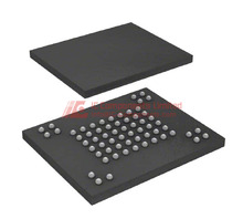
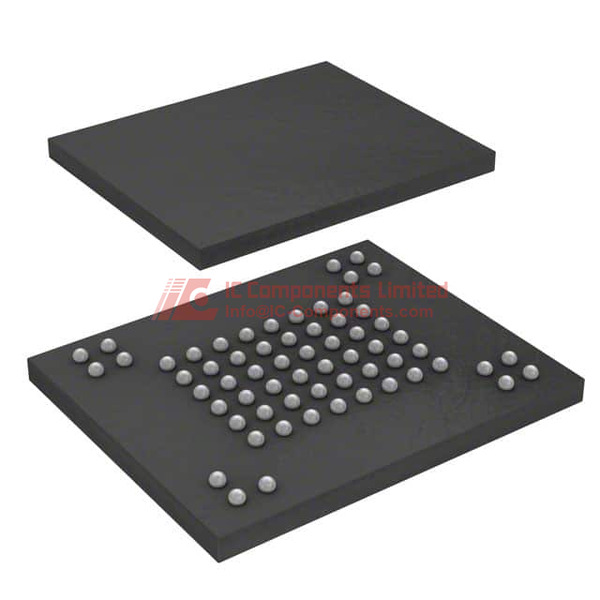
The component is housed in a space-efficient 63-BGA (11x9mm) package configuration, specifically a 63-VFBGA format, which addresses the growing demand for miniaturization in portable and embedded devices. This Ball Grid Array packaging provides excellent thermal performance and electrical characteristics while maintaining a small footprint suitable for high-density PCB layouts. The device operates reliably across an extended temperature range from -40°C to 105°C, making it suitable for industrial, automotive, and harsh environment applications where temperature variations are significant.

Key specifications include a supply voltage range of 2.7V to 3.6V, providing flexibility for integration into various power management schemes and enabling compatibility with both 3.3V and lower voltage systems. The NAND flash technology implementation offers superior endurance and data retention characteristics compared to traditional storage solutions, while the RoHS3 compliance ensures environmental responsibility and regulatory adherence for global market deployment.

Primary advantages of this memory solution include its high storage density, fast access times, low power consumption characteristics typical of NAND flash technology, and robust parallel interface that simplifies integration into existing system architectures. The surface mount technology facilitates automated assembly processes, reducing manufacturing costs and improving production reliability. The wide operating temperature range and industrial-grade specifications make it particularly valuable for applications requiring long-term reliability under challenging conditions.

Compatibility extends across numerous microcontroller and processor platforms that support parallel memory interfaces, including ARM-based systems, FPGA implementations, and various embedded controllers. The standard parallel interface ensures straightforward integration without requiring specialized controllers or complex interface circuitry, making it accessible for diverse design teams and applications.

Application areas encompass embedded systems, industrial automation equipment, automotive electronics, telecommunications infrastructure, medical devices, consumer electronics, and IoT devices where reliable non-volatile storage is essential. The device is particularly well-suited for firmware storage, data logging applications, configuration parameter storage, and any application requiring fast, reliable, and persistent data storage capabilities.

Regarding equivalent models, several alternatives exist in the market including Micron's MT29F1G08 series, Samsung's K9F1G08 family, Winbond's W29N01HV series, and Macronix's MX30LF1G18AC. Additional comparable options include Toshiba's TC58NVG0S3H, ISSI's IS34ML01G1, GigaDevice's GD5F1GQ4U series, and Alliance Memory's AS5F31G04SND. These alternatives typically offer similar capacity, interface types, and performance characteristics, though specific timing parameters, package options, and temperature ranges may vary. When considering substitutes, designers should carefully evaluate pin compatibility, timing specifications, command set compatibility, and package dimensions to ensure proper system integration and performance equivalence.

S34ML01G100BHV003 Key Technical Attributes

1Gbit Memory

NAND Flash Technology

Parallel Memory Interface

S34ML01G100BHV003 Packing Size

63-BGA package with a dimension of 11x9 mm, constructed for surface mount applications. The tape & reel packaging facilitates automated production processes. The electrical pins are organized as 128M x 8, with optimal heat dissipation supported by the 63-VFBGA (Very Fine Ball Grid Array) format. The recommended supply voltage ranges from 2.7V to 3.6V, ensuring stable operational performance across industrial environments. Operating temperature is rated for -40°C to 105°C, offering excellent thermal reliability.

S34ML01G100BHV003 Application

The S34ML01G100BHV003 NAND Flash memory is widely applied in embedded systems, industrial automation equipment, data logging devices, and networking hardware. Its parallel interface and high-speed write cycle make it suitable for intensive read/write operations in applications requiring fast memory access and large storage capacity. Its reliability in high-temperature environments expands usage to automotive sectors and mission-critical electronics.

S34ML01G100BHV003 Features

This IC combines high-density storage with fast access times, offering a 1Gbit memory size in an efficient 63-BGA package. The flash memory technology provides non-volatile storage that retains data even when power is lost, ideal for storing firmware, configuration data, and log files. The parallel interface supports rapid data throughput, and the 25ns write cycle time enables swift programming and erasure. Its RoHS3 compliance ensures environmental safety, while the robust operating temperature range guarantees functionality in harsh conditions. The advanced packaging increases pin counts for parallel data flow, reduces board space, and optimizes thermal performance. Cypress's ML-1 series incorporates enhancements for error correction, endurance, and retention, ensuring longevity in demanding use cases.

S34ML01G100BHV003 Quality and Safety Features

Complies with RoHS3 environmental standards, confirming the absence of hazardous substances. Manufactured under rigorous quality controls, ensuring reliability and durability. The wide thermal operational range and advanced error correction mechanisms help prevent data corruption and support long-term data retention. The surface-mount design offers secure attachment and enhanced resistance to vibration and mechanical stress.

S34ML01G100BHV003 Compatibility

S34ML01G100BHV003 is designed to be compatible with standard parallel NAND Flash controllers and microprocessor interfaces, supporting seamless integration into existing system architectures. The 63-BGA footprint matches typical PCB layouts in embedded and industrial designs, with pin configuration and voltage parameters aligning with common industry standards across flash memory solutions in the ML-1 series.

S34ML01G100BHV003 Datasheet PDF

Customers are encouraged to visit our website to download the most comprehensive and authoritative datasheet for the S34ML01G100BHV003. The datasheet contains detailed electrical characteristics, mechanical dimensions, pin configurations, absolute maximum ratings, and integration guidance. Obtain the official document directly from this page for complete technical assurance.

Quality Distributor

IC-Components is proud to be a premium distributor of Cypress Semiconductor products. We guarantee authentic S34ML01G100BHV003 devices, backed by professional support and rapid fulfillment. Take advantage of our competitive pricing—request a quote now on our website to secure the latest Cypress memory solutions for your project needs.

Frequently Asked Questions

What considerations should I keep in mind when integrating the Cypress S34ML01G100BHV003 1Gb NAND flash memory with a 3.3V logic system?
The Cypress S34ML01G100BHV003 operates with a supply voltage range of 2.7V to 3.6V, compatible with 3.3V logic levels. Ensure your system's I/O voltage levels are within this range to prevent data corruption or damage. Additionally, configure your FPGA or microcontroller's parallel interface to match the 128M x 8 organization and adhere to the specified write cycle time of 25ns to maintain reliable data operations.
How can I ensure reliable operation of the S34ML01G100BHV003 flash memory in industrial environments with temperature variations from -40°C to 105°C?
The S34ML01G100BHV003 is designed for industrial-grade reliability within this temperature range. To ensure longevity and stability, use proper circuit layout practices, including adequate decoupling and grounding. Be mindful of thermal management; avoid proximity to heat sources, and consider adding heatsinks or airflow if operating at high frequency or in high-temperature conditions to prevent thermal stress.
Is the parallel interface of the Cypress S34ML01G100BHV003 suitable for high-speed data transfer applications, and what are the main limitations?
The flash memory supports a parallel interface with a write cycle time of 25ns per word/page, suitable for moderate-speed applications. For high-speed data transfer, ensure that your system's data bus and controller can handle the parallel data throughput without introducing bottlenecks. Limitations include potential increased pin count and PCB complexity, which may impact signal integrity at very high transfer rates.
When replacing a different NAND flash device with the Cypress S34ML01G100BHV003, what key factors should I consider to prevent compatibility issues?
Verify that the new device matches the memory organization (128M x 8), voltage requirements (2.7V to 3.6V), and interface type (parallel). Check the packaging (63-BGA, 11x9 mm) and pin configuration to facilitate proper PCB layout. Additionally, review the device’s timing specifications such as write cycle time and ensure your controller software supports any differences in command sets or initialization procedures.
Can the Cypress S34ML01G100BHV003 flash memory be used in a battery-powered embedded system, and what are the design implications?
Yes, the device is suitable for battery-powered systems due to its low operating voltage range (2.7V to 3.6V). To optimize power consumption, implement power-down and standby modes if supported, and minimize unnecessary write cycles, as flash memory writes are power-intensive and affect battery life. Use low-leakage components and proper power sequencing to ensure data integrity during power transitions.
What are the best practices for designing a PCB layout when incorporating the Cypress S34ML01G100BHV003 63-BGA package?
Use short, well-routed signal traces with controlled impedance to preserve signal integrity. Ensure proper placement of decoupling capacitors close to the device power pins, and implement ground planes for effective noise reduction. Pay attention to BGA via stitching and maintain sufficient clearance around the BGA balls to facilitate rework if necessary. Refer to Cypress's recommended PCB layout guidelines for specific pin assignments and signal routing.
How does the Cypress S34ML01G100BHV003's RoHS3 compliance impact design considerations and environmental compliance?
RoHS3 compliance indicates the device meets environmental standards for restriction of hazardous substances. When designing your product, ensure that all components, including the S34ML01G100BHV003, are sourced from qualified suppliers providing RoHS-compliant parts. This reduces legal and environmental risks and simplifies compliance with regulations like WEEE or REACH.
What are the key factors to consider when migrating from a smaller-capacity flash memory to the Cypress S34ML01G100BHV003 in an existing design?
Confirm compatibility of the memory interface, pinout, and device package. Assess whether the existing controller supports the larger capacity (1Gb) and the specific memory organization (128M x 8). Update firmware or driver software to accommodate different command timings or addressing schemes. Also, reevaluate power supply and decoupling requirements to accommodate the memory's operational specifications.
What precautions should I take to ensure data retention and reliability of Cypress S34ML01G100BHV003 in long-term applications?
Maintain stable power supply voltages within the specified range and avoid frequent unnecessary write cycles, as flash cells have limited write endurance. Conduct regular data integrity checks if possible. Include proper error detection and correction mechanisms in your system, and avoid exposing the device to excessive temperature fluctuations outside the -40°C to 105°C range to prevent accelerated aging.
Is the Cypress S34ML01G100BHV003 suitable for use in space or radiation-sensitive environments, and what additional considerations are necessary?
The device is primarily designed for industrial and consumer applications; it is not radiation-hardened. For space or radiation-sensitive environments, consider additional shielding or selecting radiation-hardened memory components. Evaluate the device's susceptibility to single-event upsets (SEUs) and implement error correction or redundancy as needed. Consult Cypress's datasheet and application notes for detailed reliability and radiation tolerance information.

Recent Reviews

Leave Comment
Hello, you have not logged in, please log in
User Login

Forgot password?

No account yet? Register now

Tips
Please speak legally
Your email will be hidden
Please complete all required fields ( denoted with* )
Mark
5.0

You May Also Be Interested In:


S34ML01G100BHV003

S34ML01G100BHV003

Cypress Semiconductor Corp

IC FLASH 1GBIT PARALLEL 63BGA

In Stock: 16825

SUBMIT RFQ